


The ability to accurately produce and control waveforms of various frequencies and profiles has become a key requirement across a number of industries.
Whether requiring agile frequency sources that deliver low phase noise with good spurious performance for communications applications or simply generating a frequency stimulus in industrial or bio-medical applications, the ability to conveniently and cost effectively generate an adjustable waveform is an important design consideration.
Many possibilities for frequency generation are open to a designer, ranging from PLL-based techniques for high frequencies to dynamically programming the output of a digital-to-analog converter (DAC) to generate frequencies of lower values. Another technique that is rapidly gaining acceptance when solving frequency (or waveform) generation requirements both in communications and industrial applications is direct digital synthesis (DDS).
Introduction to DDS
The combination of continual process improvements and modern design techniques has resulted in DDS chips attaining power consumption levels and costs that were previously impossible for DDS-based solutions. For example, the AD9833 (a DDS-based programmable waveform generator) consumes a maximum power of 31 mW and is available in a 10-lead MSOP.
DDS devices are now available that can generate sub-Hz frequencies up to 400 MHz (based on a 1 GHz clock). The power, package, and cost benefits of new process technologies combined with the excellent performance inherent in DDS and the ability to digitally (re)program the output waveform characteristics make DDS devices an extremely attractive solution over more discrete and less flexible solutions.
Applications currently using DDS-based waveform generation can be segmented into two distinct categories. First, designers of communications systems requiring agile frequency sources with excellent phase noise and spurious performance often choose DDS for its combination of spectral performance and frequency tuning resolution. Such applications include using a DDS to enhance overall frequency tunability as a local oscillator, or even for direct transmission.
Second, many industrial and biomedical applications use DDS as a programmable waveform generator. Because a DDS device is digitally programmable, adjustments can easily be made to the phase and frequency of a waveform without the need to change any external components as is often the case with traditional waveform generators. This allows simple frequency adjustment to locate resonant frequencies or to compensate for temperature drift. Such applications include using a DDS device as a frequency stimulus to measure impedance (for example, in an impedance-based sensor), to generate pulse wave modulated signals for micro actuations, or to examine attenuation in LAN or telephone cables.
Overview
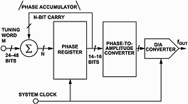
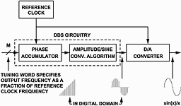
DDS is a technique using digital data processing blocks to generate a frequency and phase-tunable output signal referenced to a fixed-frequency precision clock source. In essence, the reference clock frequency is divided down in a DDS architecture by the scaling factor set forth in a programmable binary tuning word. The key blocks in most DDS solutions are the phase accumulator, phase-to-amplitude conversion block (making up the DDS core), and usually a high performance DAC that is specifically designed to work with the DDS core. In addition, phase and frequency registers or RAM may be included to allow various modulation schemes to be generated. Also, a high performance comparator to allow clock signals to be generated is often included. The tuning word is typically 24 to 48 bits long, which provides the superior frequency tuning resolution of a DDS device. A DDS device is usually programmed via a simple serial or parallel interface with some DDS designs allowing predefined frequency or phase profiles to be written to the device and activated later. An extensive review of the theory of operation and the key blocks in a DDS device are given in the next section.
Theory of operation
The main components of a complete direct digital synthesiser are a numerically controlled oscillator (NCO), frequency and phase modulators, a phase-to-amplitude converter (often a sine look-up table), and a D/A converter. These blocks are represented in Figure 1.
A direct digital synthesiser produces a sine wave at a given frequency. This frequency is dependent on two variables:
* Reference clock/master clock of the DDS device.
* Binary number programmed into the frequency register.
The binary number in the frequency register provides the input to the phase accumulator. In the case of a sine look-up table, the phase accumulator then computes an address for the look-up table. The sine value is converted to an analog value by the D/A converter. To generate a fixed frequency sine wave, a constant value (the phase increment determined by the binary number) is added to the phase accumulator with each clock cycle. If the phase increment is large, the phase accumulator will step quickly through the sine look-up table and generate a high frequency sine wave. The following sections take a closer look at the main building blocks of a DDS device.
Phase accumulator
The phase accumulator, which varies in size from 24 to 48 bits long, is the main component of the NCO. Continuous time signals have a phase range of 0 to 2 pi. Outside this range of numbers, the sinusoid functions repeat themselves in a periodic manner. The digital implementation is no different. This carry function allows the phase accumulator to act as a phase wheel in the DDS implementation.
To understand this basic function, visualise the sine wave oscillation as a vector rotating around a phase circle (Figure 2). Each designated point on the phase wheel corresponds to the equivalent point on a cycle of a sine waveform. As the vector rotates around the wheel, a corresponding output sine wave is being generated. One revolution of the vector around the phase wheel, at a constant speed, results in one complete cycle of the output sine wave. The phase accumulator is utilised to provide the equivalent of the vector's linear rotation around the phase wheel. The contents of the phase accumulator correspond to the points on the cycle of the output sine wave.
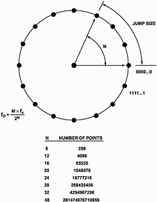
The number of discrete phase points in the wheel is determined by the resolution of the phase accumulator (N), which determines the tuning resolution of the DDS device. The output of the phase accumulator is linear and cannot directly be used to generate a sine wave or any other waveform except a ramp. A phase-to-amplitude look-up table is used to convert a truncated version of the phase accumulator's instantaneous output value into the sine wave amplitude information that is presented to the D/A converter. The AD9833 and AD9834 devices' DDS architectures exploit the symmetrical nature of a sine wave and use mapping logic to synthesize a complete sine wave cycle from 1/4 cycle of data from the phase accumulator. The phase-to-amplitude look-up table generates all the necessary data by reading forward then back through the look-up table (Figure 3).
The phase accumulator is actually a modulus M counter that increments its stored number each time it receives a clock pulse. The magnitude of the increment is determined by a binary input number or word (M) contained in a delta phase register that is summed with the overflow of the counter. The word in the delta phase register forms the phase step size between reference clock updates; it effectively sets how many points to skip around the phase wheel. The larger the jump size, the faster the phase accumulator overflows and completes its equivalent of a sine wave cycle. For an N = 28-bit phase accumulator, an M value of 0000...0001(one) would result in the phase accumulator overflowing after 228 reference clock cycles (increments). If the M value is changed to 0111...1111, the phase accumulator will overflow after only 21 clock cycles, or two reference clock cycles. This control of the jump size constitutes the frequency tuning resolution of the DDS architecture.
The relationship of the phase accumulator and delta phase accumulator form the basic tuning equation for DDS architecture:
ƒOUT = (M(REFCLK))/2N
where:
ƒOUT = output frequency of the DDS
M = binary tuning word
REFCLK = internal reference clock frequency (system clock)
N = length in bits of the phase accumulator
Changes to the value of M result in immediate and phase-continuous changes in the output frequency. No loop settling time is incurred as in the case of a PLL.
As the output frequency is increased, the number of samples per sinusoid decreases. Since sampling theory dictates that at least two samples per cycle are required to reconstruct the output waveform, the maximum DDS fundamental output frequency is REFCLK/2. However, for practical applications, the output frequency is somewhat less than that to improve the quality of the reconstructed waveform and permit filtering on the output.
Sine ROM
As stated in the previous section, the output of the phase accumulator is linear and, therefore, cannot directly be used to create a sine wave. It must be converted from phase information into a sinusoidal value. Because phase information maps directly into amplitude, the sine ROM uses the digital phase information from the phase accumulator as an address to a look-up table and converts the phase information into amplitude. The output of the phase accumulator is truncated to ~12 bits before entering the sine ROM, since using the full resolution of the phase accumulator would be impractical and unnecessary; it would require a look-up table of 2P entries, where P is the resolution of the phase accumulator. It is necessary only to have sufficient phase resolution such that the errors due to truncation are smaller than the resolution of the on-board DAC.
Digital-to-analog converter
The AD983x DDS devices come with an on-board DAC. The output of the sine ROM is fed into the DAC, which then converts the digital sine output into an analog sine wave. Some DDS devices offer the ability to configure the DAC for either single-ended or differential operation. IOUT and IOUTB can be connected through equal external resistors to AGND to develop complementary output voltages. The load resistors can be any value required, as long as the full-scale voltage developed across it does not exceed the voltage compliance range. Since RSET controls full-scale current, adjustments to RSET can balance changes made to the load resistors.
Phase registers
Many DDS devices often include additional phase register blocks. The contents of the phase registers are presented to an adder that is placed after the phase accumulator. This enables the output sine wave to be phase-delayed in correspondence with a phase tuning word. The length of the adder circuit determines the number of bits in the phase tuning word and, therefore, the resolution of the delay. This is extremely useful for phase modulation.
Conclusion
A DDS device is fundamentally a digital method of generating an output waveform and as such, benefits from the ability to digitally process the waveform. While a sine wave was used to explain the function of a DDS device, it is also possible to generate triangular or digital outputs from the AD9833 and AD9834. The combination of high spectral purity, fine tuning resolution, and digital control (allowing frequency/phase adjustment) make the DDS architecture highly suitable for many applications.
For more information contact Stephen Silberman, Analog Data Products, a division of Avnet Kopp, 011 809 6100.


© Technews Publishing (Pty) Ltd | All Rights Reserved
 printer friendly version