Tech note: How to use a FET to overcome the input voltage limitation of a linear regulator
2 June 2004
Power Electronics / Power Management
Jeff Falin, Texas Instruments
All integrated circuits have an input voltage limitation due to the manufacturing process. This limitation is cumbersome when trying to step down a high-supply voltage to a lower, regulated voltage using a DC/DC converter such as a linear regulator. Adding a FET to the input of a linear regulator creates a DC/DC converter with a wider input voltage range than the range of the regulator alone. The excess voltage (and therefore power) is dropped across the FET.
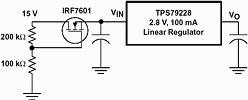
Figure 1 shows an IRF7601 N-channel MOSFET on the input of a TPS79228 2,8 V, 100 mA, low-noise, high-PSRR LDO regulator. The two resistors provide a bias voltage to the gate of the MOSFET and the load current determines the voltage at the source of the MOSFET (ie, the FETs on resistance adjusts to meet the load current). The MOSFET is selected based on three criteria: drain to source breakdown voltage, gate drive requirements, and power dissipation capabilities. In this example, the maximum power-supply voltage is 15 V, but the TPS79228 has a maximum recommended operating input voltage of 5,5 V, so a MOSFET with a 20 V breakdown voltage is selected.
Figure 1. MOSFET switch used to expand the regulator’s input voltage
To determine the minimum bias voltage for the gate of the MOSFET, the MOSFET's drain current (ID) vs gate-source voltage (VGS) data sheet curve is required. For the IRF7601, the curves indicate that the device needs VGS slightly below 1,5 V for a 100 mA output current. Since the maximum dropout of the regulator is 100 mV at 100 mA, the regulator's input voltage must stay above 2,9 V. Therefore, the gate of the MOSFET must be biased to at least 1,5 V + 2,9 V = 4,4 V, so that when the MOSFET is providing 100 mA, its source voltage does not drop below 2,9 V. The maximum gate bias voltage is simply the maximum recommended operating voltage for the regulator, or 5,5 V. This voltage provides more than enough gate drive to provide the regulator's 1 µA of quiescent current while in shutdown mode.
Although the gate can be biased between 4,4 V and 5,5 V, a bias voltage of 5,0 V is selected to account for variations in the threshold voltage. Maximum power dissipation for the FET is:
100 mA x (15 V - 2,9 V) = 1,21 W
which the IRF7601 in a Micro 8 package can handle for TA = 55°C.
So, a low noise, low ripple 2,8 V output voltage is generated from a 15 V supply using the TPS79228 and a MOSFET.
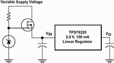
Figure 2 is slightly more complicated but may be necessary if the input voltage varies significantly. A Zener diode replaces the bottom resistor in Figure 1 and provides a fixed gate drive to the MOSFET. The output voltage of the Zener is selected in a manner similar to that explained previously.
Figure 2. MOSFET switch biased with Zener diode used to expand regulator’s input voltage
Summary
Either method is acceptable for creating a DC/DC converter with a wider input voltage range than the converter IC allows. The single MOSFET solution is the simplest and cheapest solution. The MOSFET biased with a Zener diode is the best choice when the supply is unregulated.
Further reading:
12 kW hybrid inverter
Power Electronics / Power Management
Sungrow recently unveiled its next-generation residential energy storage solution, expanding its power range from 5 kW to 12 kW with the introduction of the new MG12RL hybrid inverter.
Read more...
40 W and 75 W railway DC/DC converter
Brabek
Power Electronics / Power Management
RECOM has announced two new cost-efficient DC/DC converters for the rail market with an ultra-wide 11:1 input range to cover all nominal input voltages from 24 to 110 V DC.
Read more...
Power modules for solid-state transformers
RS South Africa
Power Electronics / Power Management
Microchip’s new 3,3 kV silicon carbide modules deliver the required thermal performance and efficiency for SSTs to increase power available for token generation.
Read more...
Solving South African power problems with locally built intelligence
Editor's Choice Power Electronics / Power Management
Smart metering infrastructure in South Africa remains patchy. The rollout has been slow, coverage is inconsistent, and for the most part, granular per-unit measurement simply does not exist.
Read more...
Wide range power module
Power Electronics / Power Management
The latest DC-DC modules from Würth Elektronik are characterised by high resilience to voltage transients on the 24 V bus and an extremely wide input-voltage range from 3,5 V to 38 V.
Read more...
Selecting primary batteries for maximum service life
Uniross Batteries
Power Electronics / Power Management
Primary batteries play an important role in IoT applications. Designed for longevity, they have a high-energy capacity and are often used in standalone applications where charging is impractical or impossible.
Read more...
4 kW e-mobility DC-DC converter
Brabek
Power Electronics / Power Management
The RECOM RMOD4000 series of compact, plug-and-play DC-DC converters is a cost-effective solution to provide isolated 14 V, 28 V, or 56 V DC network rails from a high input voltage between 180 and 950 V DC.
Read more...
Aluminium case upgrade boosts performance
Vepac Electronics
Power Electronics / Power Management
The SQBF Quarter Brick 300 W DC to DC Converter is now available in a newly upgraded metal case designed to deliver improved durability and superior electrical performance across demanding applications.
Read more...
Extending the range of power converters
RS South Africa
Power Electronics / Power Management
Power Integrations recently announced a breakthrough in flyback topology extending the power range of flyback converters to 440 W - well beyond the limits that traditionally required more complex resonant and LLC topologies.
Read more...
Power-dense modules operate up to 115 V DC
Brabek
Power Electronics / Power Management
The RPMVH-0.5 series of cost-effective, non-isolated buck regulator modules from RECOM delivers 0,5A of output at fully regulated voltages up to 24 V DC.
Read more...


 printer friendly version