


Texas Instruments announced a massive expansion of its MSP430 microcontroller family. The first new devices introduce the company's smallest, low power MCUs ever - the MSP430F20xx MCU series - with 4 x 4 mm² and 16 MIPS of 16-bit performance.
Overview
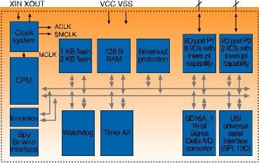
The MCU platform MSP430F20xx is equipped with a modern 16-bit RISC CPU. The orthogonal architecture provides the flexibility of 16 fully addressable, single-cycle 16-bit CPU registers and the power of a RISC. The modern design of the CPU offers versatility through simplicity using only 27 easy-to-understand instructions and seven consistent addressing modes. This results in a 16-bit low power CPU that has more efficient processing, is smaller-sized and highly code-efficient. Now it is possible to develop new ultra-low-power, high-performance applications at a fraction of the code size. The following attributes of the modern CPU should be mentioned: a large register file eliminates the accumulator bottleneck; optimised for C and assembler programming; compact core design reduces power; up to 16 MIPS of performance available.
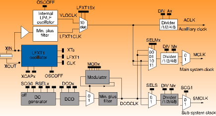
The improved digitally-controlled oscillator (DCO) allows a flexible clock system operation up to 16 MHz with no external components. The MSP430 clock system is designed specifically for battery-powered applications. The recently-announced MSP430F20xx family operates with a very low active current of 200 μA per MIPS. Multiple oscillators are utilised to support even-driven burst activity. A low-frequency auxiliary clock (ACLK) is driven directly from a common watch crystal. The ACLK can be used for a background realtime clock self-wake-up function. The master clock (MCLK) will be driven by the DCO.
The master clock is used by the CPU and from the high-speed peripherals, for example sigma-delta converter and the universal serial interface. The DCO is active in less than 1 s and stable over temperature and voltage. All these advantages make the clock system very flexible. The DCO offers a range from 400 kHz up to 16 MHz, the low-frequency and very low frequency oscillator operating range is 10 kHz up to 50 kHz and 4 kHz up to 20 kHz. Figure 2 shows the F20xx clock block diagram.
Details
All MSP430F20xx devices offer an in-system programmable flash for greater design flexibility, field upgrade and elimination of external EEPROMS. MSP430F200x MCUS have 1 KB flash and the MSP430F201x series 2 KB flash. All MCUs of the F20xx family are equipped with the same RAM size. 128 byte of RAM, when combined with a full-featured CPU, allows full development in the program language C. A further improvement of the in-system programmable flash is the smaller 64 byte segments. Thanks to these small segments the programming time is as fast as 17 μs per byte. The programming voltage drops down to 2,2 V. The flash memory can be programmed via JTAG port, the bootstrap loader, or in-system by the CPU. The CPU can perform single-byte and single-word writes to the flash memory. A zero-power brown-out reset (BOR) function and an enhanced watchdog timer enhance reliability. The primary function of the watchdog timer (WDT+) module is to perform a controlled system restart after a software problem occurs. If the selected time interval expires, a system reset is generated. If a watchdog function is not needed in an application, the module can be disabled or configured as an interval timer and can generate interrupts at selected time intervals. The brown-out circuit is implemented to provide the proper internal reset signal to the device during power-on and power-off. All the fail-save features of MSP430F20xx devices are available during all modes of operation with no power penalty.
All MCUs of the new family are equipped with 10 general-purpose input/output pins (I/Os). There is one 8-bit I/O port P1 implemented and two bits of I/O port P2. All individual I/O bits are independently programmable and any combination of input, output, and interrupt condition is possible. To further reduce system cost, all 10 GPI/O pins include pull-up/pulldown resistors to eliminate additional external components. As the need for low pin-count devices increases, it is critical to minimise overhead pins associated with debug, test and emulation. The typical JTAG interface used on the MSP430 products uses either four or five device pins depending on the product family. In order to save on device pins, the previous lower pin-count devices have used multiplexing of this interface with functional pins. Although this reduces pin-count, it does not allow the functional pins to be available during debug or emulation. This being the case, a simple, two-wire interface is being proposed. The improved JTAG interface module allows a two-wire communication called SPY bi-wire function. This new interface works with only two pins. But the new JTAG module is compatible to former JTAG modules. Easy debug commands can be used in SPI bi-wire mode like breakpoint commands and program single-stepping. To accelerate F20xx MCU design-in, designers can begin development with TI's new existing MSB430 JTAG pods that support the new SPY bi-wire interface.
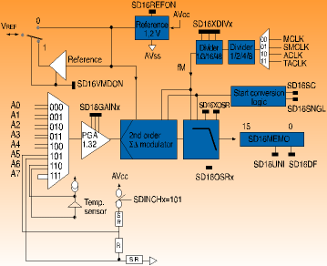
Several high-performance ADCs are available in the MSP430F20xx family: a slope ADC, a 10-bit SAR ADC and a 16-bit sigma-delta ADC. For example, the MSP430F2003 and F2013 are equipped with the sigma-delta converter SD16_A. The SD16_A module is a single 16-bit, sigma-delta analog-to-digital conversion module with a large dynamic input range and an internal voltage reference. It has up to eight fully-differential multiplexed inputs, including a built-in temperature sensor. The converter is based on a second-order oversampling sigma-delta modulator and a digital decimation filter. The decimation filter is a comb-type filter with selectable oversampling ratios from 32 up to 1024. The analog-to-digital conversion is performed by a 1-bit, second-order sigma-delta modulator. A single-bit comparator within the modulator quantizes the input signal with the frequency fM. The resulting 1-bit data stream is averaged by the digital filter for the conversion result. The full-scale input voltage range for each analog input pair is dependent on the gain setting of the programmable gain amplifier (PGA) of each channel. The maximum full-scale range is ±VFSR where VFSR is defined by:
VFSR = (VREF/2)/(GAIN PGA)
For 1,2 V reference, the maximum full-scale input range for gain of 1 is:
±VFSR = (1,2 V/2)/(1) = ±0,6 V
The SD16_A module has a built-in 1,2 V reference. It is enabled by setting the SD16REFON bit. When using the internal reference, an external 100 nF capacitor connected between is VREF pin (P1.3) and VSS. The internal reference voltage can be used off-chip when SD16VMIDON = 1. An external voltage can be applied to the VREF pin input when the SD16REFON and SD16VMIDON are both reset. In the control register SD16CTL, both bits SD16REFON and VMIDON can be configured.
The SD16_A module can have up to eight differential input pairs multiplexed into the PGA. Up to five pairs (A0...A4) are available externally on the low pin-count device. An internal temperature sensor is available by using the A6 multiplexer input. Input A7 is a shorted connection between the + and - input pair and can be used to calibrate the offset of the SD16_A input stage.
Conversion mode and conversion memory register
The module can be configured for two modes of operation, single- and continuous-conversion.
The single conversion is converted once per the channel, and in continuous mode the channel will be converted continuously. The SD16MEM0 register is associated with the SD16_A channel. Conversion results are moved to the SD16MEM0 register with each decimation step of the digital filter. The SD16IFG bit is set when new data is written to the memory. The interrupt flag is automatically cleared when SD16MEM0 is read by the CPU or may be cleared with software. The single or continuous mode can be configured in the control register SD16CCTL0 (bit-10).
The output data format is configurable in two's complement, offset binary or unipolar mode. The data format is selected by the SD16DF and SD16UNI bits.
All MCUS of the F20xx family are equipped with a 16-bit timer with two capture/compare registers. Above that the MSP430F20x2 and F20x3 include a universal serial interface (USI) that can be configured for either I²C or SPI master or slave communication. The configuration is selectable with the control registers USICTLO and USICTL1. As example, the USI module is configured as SPI master by setting the master bit USIMST and clearing the I²C bit USII2C. Since the master provides the clock to the slave(s), an appropriate clock-source needs to be selected and the SCLK must be configured as output. The two main building blocks of the USI module are the shift register and the bit counter. The shift register, USISR, is directly accessible by the software and contains data to be transmitted or data that has been received. The bit counter counts the number of sampled bits and sets the USI interrupt flag USIIFG whenever USICNTx value transitions to zero, either by counting or directly writing to it. Writing a value >0 to USICNTx automatically clears the USI interrupt flag, when USIIFGCC = 0. Both the counter and the shift register are driven by the same shift clock.
The USI module offers the following features:
SPI_Mode:
* Three-wire SPI mode support.
* 8-bit or 16-bit shift register.
* MSB or LSB first.
* Slave operation in LPM4, hence no internal clock required.
I²C_Mode:
* Start and stop condition detection.
* +SCL is held low after start condition detection.
* Arbitration lost detection in master mode.
* Slave operation in LPM4, hence no internal clock required.
If a small software is written, the USI module can be used as UART or LIN module, too.
Summary
Ultra-low-power consumption, high-performance 16-bit architecture, powerful peripherals, a very flexible clock system and a low pincount, all these features are very necessary in portable consumer and industrial applications. The MSP430F20xx MCU platform is designed for systems with ultra-low-power and high performance analog requirements. Applications such as fire and motion detectors are typically for microcontrollers of the MSP430F20xx platform. All applications designed with F20xx feature good battery utilisation and long standby.


© Technews Publishing (Pty) Ltd | All Rights Reserved
 printer friendly version