


Printed circuits boards (PCBs) used in the electronics world are sometimes produced by an electroplating process. Electroplating is the electrochemical process of depositing a metallic coating on a material of an object. When it is immersed in a plating solution, a low voltage electric current flows through it, causing the metallic coating to be attracted to the object to be plated.
Measurement of current plays an important part here in this process to ensure quality of the finished PCBs, eg, the structure, thickness of the tracks, and also, saves time in production.
LEM's LF Series compact AC/DC current transducers are highly useful in this application as the power supplies or special rectifiers involved in the electroplating process are often purpose-built. The LF models cover the nominal measuring range of 100, 200, 300, 500, 1000 and 2000 A rms, each offering a similar shape, with different sizes rated to their dedicated nominal current measuring capacity. The LF Series additionally has flexible mounting, and all models can be fixed either vertically or horizontally.
There are different ways to do the electroplating:
* With a DC plating current: The most conventional - the object to be plated is located on the cathode linked to the negative pole of the battery. The metal to be deposited is installed on the anode, which is linked to the positive pole of the battery. The cathode, anode and their associated objects are immersed into a salt solution of the plating metal. The electrons of the solution circulate through the battery and accumulate on the cathode, where the positive ions of the metal in the solution are attracted to it. As the object to be plated is negatively loaded the positive metallic ions accumulated on it produce the desired metallic plating (Figure 1a).
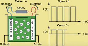
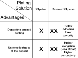
* With a DC pulse plating current: This plating follows the same previous principle, except that the metal deposition is ensured by pulsed electrolysis. An interrupted (square pulse) DC current of equal amplitude and duration with a certain duty cycle is used to facilitate the electroplating process. Using a pulsed DC current causes a higher voltage vs. the steady DC plating. This directly improves the plating deposit quality. (Figure 1b and Table 1)
* With a reverse DC pulse plating current: This is an expanded system of the previous pulse plating process. Amplitudes, frequency, duration and polarity of the DC pulses series can vary under full control.
Typical currents used are 200, 400, 600, 1200 A d.c. with a three times higher in amplitude reverse DC current (Figure 1c). This leads to faster and a higher quality production of PCBs (Table 1).
When tracks are bigger than through-holes on PCBs, it becomes difficult to ensure an efficient and uniform copper deposit. Copper ions are attracted to where the current density is high, such as on the edges of the holes. Conversely, they avoid the deep through-holes where there is a low current density. This results in more copper on the edges of the holes than in the holes. Using a lower current density is a solution, but leads, however, to a longer process time. Also, a too low current can produce coarse copper in the holes resulting in some cracking. Reverse pulse plating completed with an appropriate electrolyte is the answer. The reverse current creates a 'shield' on the sensitive areas (edges or through holes). With the positive pulse, the shield disappears progressively on the protected areas when the deposit begins on the unshielded areas. This leads to less deposit on these sensitive areas than on the other ones. By this way, copper deposit of uniform thickness through the holes and at their edges is ensured.
To produce these different plating currents, special rectifiers have been designed. However, due to the impedances (resistance, inductance and capacitance) of the external cabling and electrolytic solution, if no precautions are taken the pulse characteristics will be affected, resulting in overshoot and/or undershoot.
To ensure the best plating process and quality, the pulse current waveform should stay stable and similar to the initial adjusted value regardless of the load. Then, the overshoot or undershoot must be avoided or compensated for. Rise and fall times of the direct and reverse pulse currents are also decisive on the quality of the plating. With a closed loop control system, the current pulse waveform of the rectifiers can continuously be monitored and adjusted with the help of current transducers such as one of LEM's LF series transducers. The LF series provides a quick response time (in less than 1 µs) at 90% of the nominal current, allowing a realtime control of the rise and fall times of the current pulses of the rectifiers.
Other features of the LF series include: bipolar AC and DC current measurement; ±0,3 % typical accuracy at 25°C at nominal current; bipolar ±12 to 24 V d.c. power supply; galvanic isolation; EN 50178 compliance.
| Tel: | +27 11 626 2023 |
| Email: | [email protected] |
| www: | www.denver-tech.co.za |
| Articles: | More information and articles about Denver Technical Products |


© Technews Publishing (Pty) Ltd | All Rights Reserved
 printer friendly version