


Successive approximation algorithm (CSA) is Cypress Semiconductor’s new capacitive sensing algorithm for its CY8C20x34 PSoC device family.
CSA enables the implementation of an array of capacitive sensors through switched capacitor circuitry, an analog multiplexer and digital counting functions. The hardware configuration works in conjunction with high-level software routines from the CSA User Module found in PSoC Designer to compensate for environmental and physical sensor variations.
What is capacitive sensing?
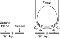
A capacitive sensor is a pair of adjacent electrodes (Figure 1). When a conductive object is placed in proximity of the two electrodes, the capacitance is changed. The base capacitance is often referred to as the parasitic capacitance (CP). The physical sensor itself is typically a copper trace constructed on a PCB. Sensors can be any conductive material. For example, one could use indium tin oxide (ITO) and print the pattern on a transparent substrate.
What is successive approximation?
The successive approximation method, developed by Cypress, uses the PSoC's switched capacitor circuitry to convert capacitance into a voltage. The voltage is then measured using a counter and a single-slope ADC. The capacitance measurement is achieved by converting the capacitance to its equivalent resistance, using the equivalent resistance to set and maintain voltage on a capacitor, then measuring the sampled voltage using an adjustable current source.
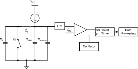
In addition to the sensor capacitor, CSA uses an internal capacitor (CInternal) and an optional external modification capacitor (CMod). The block diagram for CSA appears in Figure 2.

The circuitry brings the sensor capacitor to a voltage relative to the capacitance of the sensor. The PSoC's internal main oscillator (IMO) clocks the switched capacitor.
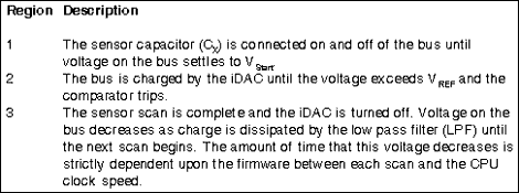
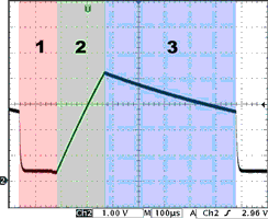
To fully understand how CSA functions, it is useful to look at the actual waveforms of CSA. Figure 3 shows the CSA waveform seen by probing CMod in a project with a single sensor and no finger present. Three regions can be seen in the CSA waveform. Table 1 describes the regions that can be seen in Figure 3. Each region is described in more detail in the following sections.
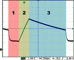
Region 1
In Region 1 of the CSA waveform the sensor capacitor (CX) is connected to the analog global bus, then grounded, in alternating phases. During Phase 1 (φ1), CX is connected in the analog global bus in parallel with CMod and CInternal. The block diagram of Phase 1 is shown in Figure 4. CInternal and CMod share charge with CX. Charge continues to flow onto CMod and CInternal from the iDAC current source. Phase 2 (φ2) disconnects CX from the analog global bus and discharges CX by connecting it to ground, leaving only CMod and CInternal connected. This is shown in Figure 5.
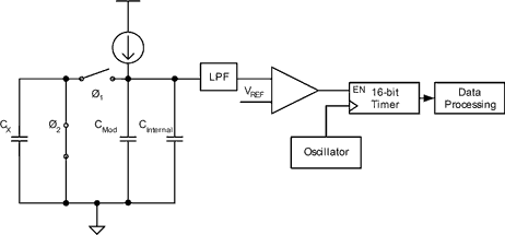
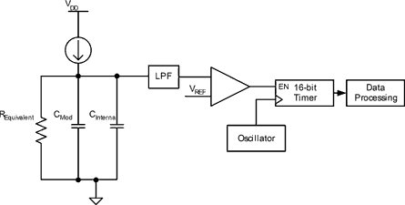
CX is an effective resistance to ground through Phases 1 and 2. An equivalent block diagram is shown in Figure 6. The equivalent resistance is given by:
REquivalent = 1/fS · CX ………………… Equation 1
where: fS is the switching frequency of Phases 1 and 2; CX is the sensor capacitance.
The constant iDAC current flows through this resistance resulting in a voltage, VStart. VStart is given by:
VStart = (1/fS · CX) iDAC ………………… Equation 2
where: iDAC is the iDAC current, VStart is set to a value below VREF with the switched capacitor circuit running. This is accomplished by tuning the iDAC through successive approximation, which uses a binary search to determine the appropriate iDAC setting. Once the bus has been charged to VStart, the iDAC current setting that was used is stored, and the process is repeated for each sensor in the project.
Region 2
After the voltage on CMod and CInternal settle to VStart, the measurement sequence begins. A counter clocked by the IMO is enabled. As the counter runs, the iDAC charges CMod and CInternal until the voltage on the capacitors reaches VREF. At VREF, the comparator disables the counter. The number of IMO clock cycles (referred to as counts) recorded by the counter is used to determine if a finger is present on a sensor. Counts are taken after each measurement sequence and compared to the baseline count number, a stored value with no finger present on the sensor. If the difference between the recorded counts and the baseline counts exceeds the finger threshold value, sensor activation is detected.
The presence of a finger on the sensor increases the capacitance (CX) of the sensor, which decreases the equivalent resistance (REquivalent) formed by the switching of φ1 and φ2. This is evident in Equation 1. The lower resistance results in a lower voltage across the capacitors (CMod and CInternal), which we will call VFinger. Thus, it will take longer for the iDAC to charge the voltage on the bus from VFinger to VREF than it does from VStart to VREF. This results in more counts (ie, object present) on the sensor. A graphical representation of the charge time on the bus with a finger present versus not present is shown in Figure 7. The waveform in Figure 8 shows the CSA waveform with a finger present, and verifies the longer count time by the counter.
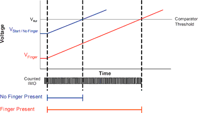
In Figure 8, the starting voltage in region 1 has dropped. This is due to the decrease in equivalent resistance, which itself is a result of the finger capacitance (CF) added in parallel with the sensor capacitance (CX). The charge time in region 2 is longer, resulting in more counts on the counter compared to no finger present on the sensor. An increase in charge time can be seen by comparing Figure 3 and Figure 8.
Region 3
In Region 3 of the waveform, the scan is complete and the iDAC is turned off. The voltage on the bus begins to drop due to charge dissipation by the Low Pass Filter (LPF) on the capacitor's input. The LPF is present to prevent the input of high frequency noise to the comparator. This voltage continues to decrease until the next scan sequence when the voltage is reset to VStart. The amount of time that the voltage spends decreasing, depends upon the firmware executed between each scan and the CPU clock frequency. A faster CPU clock frequency results in a smaller decrease in the voltage on the bus in Region 3.
Noise immunity
CSA offers high noise immunity, resulting in excellent sensitivity. Sensitivity is proportional to signal-to-noise ratio (SNR) levels. The switching of the sensor capacitor in CSA reduces the outside noise sources on the sensor capacitor that could inadvertently couple directly into the system. During Phase 2, any noise introduced through the sensor capacitor is shorted directly to ground. In addition, the grounding of the sensor capacitor reduces the input impedance of the CSA system. The lower input impedance results in smaller voltages entering the CSA system as a result of any noise current.
The input of the comparator for CSA includes an internal LPF to reduce the effect of high frequency noise on sensor scans. External to the PSoC, an optional bus modification capacitor (CMod) further improves noise performance by acting as a bypass capacitor. The bypass capacitor prevents erroneous device interrupts by eliminating large voltage swings on the device inputs.
Summary
The PSoC Mixed-Signal Array is a configurable array of digital and analog resources, Flash memory, RAM, an 8-bit microcontroller and several other features. These features allow PSoC to implement innovative capacitive sensing techniques in its CapSense portfolio. PSoC's intuitive development environment can be used to configure and reconfigure the device to meet design specifications and specification changes. Successive Approximation exhibits exceptional sensitivity and noise immunity, low power consumption and a fast update rate, along with the flexible design process inherent to the PSoC.
For more information contact Lambert Colyn, Arrow Altech Distribution, +27 (0)11 923 9600, [email protected]
| Tel: | +27 11 923 9600 |
| Email: | [email protected] |
| www: | www.altronarrow.com |
| Articles: | More information and articles about Altron Arrow |


© Technews Publishing (Pty) Ltd | All Rights Reserved
 printer friendly version