


Hot mustard – most of us have experienced that burning sensation up our nose, followed by aching eyes and a sudden flow of tears. Yes, life teaches us many lessons.
Having learnt that lesson the hard way, I swore never to touch the stuff again.
Funny how life teaches us so many lessons every day. Every awful experience often leads to lessons worth remembering for life. In electronics hardware design too, learning the 'hard way' not only results in smoke up the nose, but often lots of tears and torn wallets.
A component in every electronics system that is always a critical factor between a successful and not-so-successful product is the printed circuit board (PCB). We have all seen the PCB design landscape change dramatically in recent years. Gone are the days when a PCB was viewed merely as an interconnect platform for components, without regard for the board's importance to the overall system. The constant demand for smarter, faster, smaller, cheaper products is pushing the boundaries, if not exceeding the limits of traditional board design. And we can no longer ignore the impact of rapidly advancing programmable device technology on board layout. Far too many companies have closed doors because of incorrect PCB layout or assembly.
Today's product developers face enormous challenges as the speed and complexity of electronic designs continue to climb. Modern printed circuit designs are a far cry from the 'dot and tape drawing board' design methods that were employed from the 1960s onward. Not only are companies forced to employ sophisticated computer-aided engineering tools and analysis software, but also need the services of competent and experienced CAD engineering staff to drive these tools and apply these technologies.
Key design concerns such as skew, jitter, cross-talk, skin-effect, and high-speed propagation are no longer the domain of engineers only. Every PCB designer has to be ready to design products that continue to meet the evolving demands of technology - and customers.
Over the past few years many designers and engineers have become aware of the need to control schematic-level circuit design as well as PCB design to maintain functionality of digital circuits that host high-speed signals. High-speed signals have very fast rising and falling edges during transition from a logical 0 to a logical 1 and vice versa. Circuits with high clock rates must have fast rise and fall time signals to prevent timing violations but fast rise and fall time signals are not always clocked at high rates. Since most new ICs have rise and fall times shorter than 2 ns, many designers today are stuck with high-speed concerns even though their circuits are clocked in the lower MHz range.
Having burnt my fingers over the years, some useful design rules have become ingrained in my subconscious. Here are some of them for the benefit of those who have not tasted hot mustard yet.
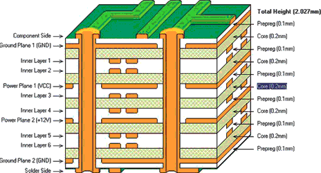
Ground planes
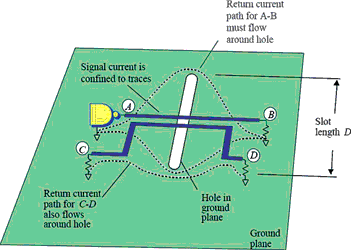
Ground planes provide stable reference voltages for exchanging digital signals and controls crosstalk between signals. Always alternate the direction of signal traces on adjacent layers. Ensure that your ground and power planes are as solid as possible, because at high frequencies, current follows the path of least inductance. Slots in a ground plane create unwanted inductance, slow down rising edges, and create mutual inductive crosstalk.
Crosstalk
The good news is that you do not have to get bogged down with equations to prevent crosstalk problems. Here are several crosstalk reduction techniques. Always try to reduce the lengths of high-frequency traces as much as possible, possibly routing them first to ensure the shortest length. Increasing the separation between traces reduces the cross-coupling between them. The greater the separation, the less the crosstalk. Decrease the loop sizes by keeping high-frequency traces closer to the ground planes. Add a grounded guard/shield trace around critical signals. Sprinkle around lots of ground vias, allowing return signal currents to flow through these as they follow the contorted path of each signal trace.
Of course not every PCB falls within the 'Black Magic' arena, as well-respected high-speed expert Howard Johnson describes it. Sometimes designers taste the hot mustard because of trial and error, and simply because they do not have anybody to really get advice from.
I just enjoyed reading the latest Popular Mechanics magazine, and therein it mentions that it took 300 years for man to prove on the moon Galileo's theory that 'gravity accelerates all objects equally, regardless of their masses or the materials from which they are made'. When Dave Scott dropped both a feather and a hammer on the moon in 1971, both reached the moondust at the same time. Sadly we do not have that luxury called time to prove our theories and designs.
A fine aid to give PCB designers the competitive edge is the internationally recognised IPC Certified Interconnect Designer (CID) qualification. The course is aimed at existing PCB design professionals who need recognition of their skills and confirmation that the knowledge they have gained through experience adheres to widely accepted standards for PCB design. The course is also aimed at companies that wish to achieve recognised international design standardisation in printed board design, printed board assembly and related design technologies. The IPC Designer Certification reinforces the knowledge gained by professionals over their many years of experience and good working practices. The programme assesses a designer's knowledge of how to transform a schematic into a reliable rigid PCB design, which can be easily manufactured, assembled and tested. IPC Designer Certification leads to probably the most respected set of formal PCB design qualifications worldwide and is the entry point into the Designer Certification Programme.
Here is to Galileo: "Well done". And also to every passionate designer who continues to be a driving force in electronics, dedicated to providing systems that not only serve our current design needs, but also help to navigate fundamental changes towards progress.
For more information contact Nechan Naicker, EDA Technologies, +27 (0)12 653 3323.
| Tel: | +27 12 665 0375 |
| Email: | [email protected] |
| www: | www.edatech.co.za |
| Articles: | More information and articles about EDA Technologies |


© Technews Publishing (Pty) Ltd | All Rights Reserved
 printer friendly version