


Cypress' CapSense Sigma-Delta algorithm
CapSense Sigma Delta algorithm (CSD) is Cypress Semiconductor's latest capacitive sensing algorithm for the CY8C21x34 and CY8C24x94 PSoC device family. CSD enables the implementation of an array of capacitive sensors through switched capacitor circuitry, an analog multiplexer, digital counting and PWM functions. The hardware configuration works in conjunction with high level software routines from the CSD User Module found in PSoC Designer to compensate for environmental and physical sensor variations.
What is capacitive sensing?
A capacitive sensor is a pair of adjacent electrodes (Figure 1). When a conductive object is placed in proximity of the two electrodes, the capacitance changes, sending a signal from the sensor to the microcontroller and allowing the intended response to occur. The base capacitance is often referred to as the parasitic capacitance (CP). The physical sensor itself is typically a copper trace constructed on a PCB, although sensors can be any conductive material. For example, one could use the transparent conductor indium tin oxide (ITO) and print the pattern on a transparent substrate.
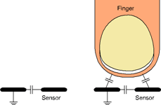
Each sensor is a capacitor with one contact grounded, and the other contact connected to the PSoC's analog global bus. The result is an active variable capacitor, CX (CX = CP + CF). The presence of a conductive object (such as a finger) increases the capacitance of the sensor with reference to ground.
Determining sensor activation is then a matter of measuring the change in capacitance.
What is Sigma-Delta?
The CSD algorithm uses the switched capacitor circuitry to convert the sensor capacitance into a voltage, which is compared to a reference voltage. When the capacitor voltage reaches the reference voltage, the comparator triggers a bleed resistor, discharging the capacitor. After the capacitor voltage discharges below the reference voltage, the bleed resistor is left floating to allow the capacitor to continue charging.
The comparator output becomes a bit-stream as it toggles the bleed resistor and manipulates its input voltage. This bit stream is logically ANDed with a PWM to provide consistent stream framing. The number of counts in each frame is analysed to determine if the capacitive sensor was activated.
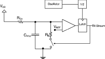
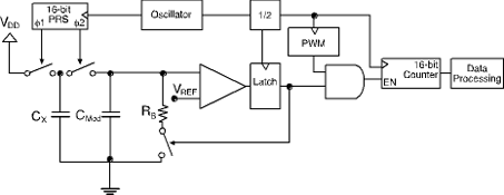
CSD requires the use of an external modulation capacitor (CMod) and bleed resistor (RB) in addition to the sensor capacitor (CX). Figure 2 shows the input stage for CSD.
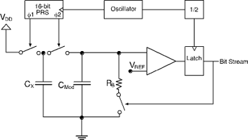
The input stage of the CSD algorithm starts with a switch capacitor network. The network starts with a switch capacitor block connected to VDD. The sensor capacitor (CX) is connected to the bus and in parallel with the required external modulation capacitor (CMod). The switch capacitor block is controlled by a 16-bit pseudo random sequencer (PRS). A PRS is used instead of fixed clock source to attenuate emitted noise on CX by reducing the amount of EMI created by a fixed frequency source and to increase EMI immunity from other sources and their harmonics.
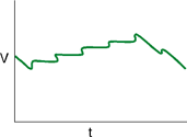
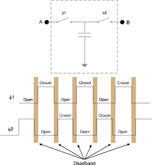
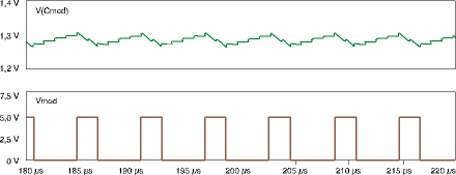
The voltage on the external modulation capacitor CMod is continually charged in small increments due to continuous operation of the switch capacitor, as shown by Figure 3. The switch capacitor causes these small voltage increments instead of a smooth increase due to its functional nature. As Figure 4 shows, phase 1 (Φ1) and phase 2 (Φ2) of the switch capacitor are never closed at the same time. Therefore, as phase 1 of the switch capacitor closes, it charges CX. As phase 1 opens, the charge on CX is held until phase 2 closes, sharing charge from CX with CMod. Because the switch capacitor is controlled by the PRS, each incremental step is not uniform in voltage or duration. These minute inconsistencies do not affect the performance of the CSD algorithm.
When the voltage reaches VREF the comparator trips, but the latch does not toggle until two clock cycles later. This is due to the latching being clocked at half the speed of the oscillator, which also clocks the PRS. It is known that the latch toggles two cycles after the comparator trips since phase 2 of the switch capacitor and the checking of the latch start on the same cycle. Therefore, the latch waits two cycles before checking again after the comparator trips. This allows for a known time between the tripping point and the latch toggle. This two cycle delay is illustrated in Figure 5.
When the latch output goes high, the switch is closed, connecting the bleed resistor (RB) to ground, which discharges CMod. Note that the waveform in Figure 3 shows that CMod is actually charged for several short moments during the discharge phase. This happens because the switch capacitor continues to operate and is dumping charge on CMod as it is being discharged.
Once again, this does not adversely affect operation. After CMod discharges beyond VREF, the latch does not toggle until after two clock cycles. Therefore, two known times exist: two clock cycles after CMod increases over VREF and two clock cycles after CMod decreases beneath VREF; the difference between these two times allows the user to know of a finger's presence. This charging and discharging with a comparator and latch is a form of Sigma-Delta modulation and is where CSD derives its name.
The switch capacitor block, when running, functions as a resistor as shown in Figure 6. The equivalent resistance is calculated by:
When a finger is present on CX, the equivalent resistance decreases. This decreased resistance causes an increase in the current flowing through RCx. To maintain the voltage on CMod near VREF, the switch connecting the bleed resistor (RB) to ground is closed with a higher duty cycle. Discharging takes longer because the voltage is still applied as it is discharging.
Bit stream filter
The opening and closing of the latch by the output of the comparator creates a variable duty cycle bit stream used to determine the presence of a finger on CX. Figure 7 shows a block diagram of a bit stream filter that takes the output from the latch and processes it.
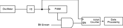
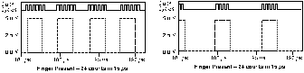
The bit stream is first ANDed with a PWM, which is clocked at the same frequency as the latch, to create measurement windows as shown in Figure 8. These measurement windows are fed directly into the enable input in a counter, which is also clocked at the same frequency as the latch. As each bit from a measurement goes into the enable input, the counter records the number of clock cycles that occur during its length.
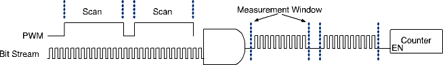
Since the duty cycle of the bit stream increases with higher capacitance, more counts are measured when a finger is present, as shown in Figure 9. The counter only records the number of clock cycles for one measurement window at a time as the PWM resets the counters by setting an interrupt when transitioning from high to low.
The raw number of clock cycles (counts) from the counter are updated to a register used by the CSD algorithm for determining a finger's presence, as well as setting the baseline and adapting to environmental conditions. The CSD algorithm looks at several measurement windows for each sensor depending on user settings.
Summary
The PSoC mixed signal array is a configurable array of digital and analog resources, Flash memory, RAM, an 8-bit microcontroller and several other features. These features allow PSoC to implement innovative capacitive sensing techniques in its CapSense portfolio. PSoC's intuitive development environment can be used to configure and reconfigure the device to meet design specifi-cations and specification changes. CapSense Sigma Delta exhibits exceptional sensitivity and noise immunity, low power consumption and a fast update rate, along with the flexible design process inherent to the PSoC.
For more information contact Arrow Altech Distribution, +27 (0)11 923 9600, [email protected], www.arrow.altech.co.za, Avnet Kopp, +27 (0)11 809 6100, [email protected], www.avnet.co.za, Future Electronics, +27 (0)21 421 8292, [email protected], www.futureelectronics.com
| Tel: | +27 11 923 9600 |
| Email: | [email protected] |
| www: | www.altronarrow.com |
| Articles: | More information and articles about Altron Arrow |
| Tel: | +27 21 421 8292 |
| Email: | [email protected] |
| www: | www.futureelectronics.com |
| Articles: | More information and articles about Future Electronics |


© Technews Publishing (Pty) Ltd | All Rights Reserved
 printer friendly version