


Today’s portable product designs put conflicting requirements on the batteries that power them. Higher feature content increases energy requirements, while end users demand long battery life.
But ever-smaller product form factors and cost constraints prevent any increase in battery capacity, so energy efficiency is paramount. The traditional approach to minimising energy consumption has been to minimise current drain; however, the energy capacity of a battery is the product of voltage, current and time, and all three variables must be addressed to achieve meaningful improvements in overall energy efficiency.
Microcontroller-based systems powered by user-replaceable batteries can benefit from an MCU that is designed to address each variable, utilising features such as on-chip voltage conversion while supporting traditional low-power operating modes.
Battery characteristics
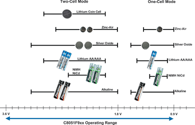
The majority of mid- to low-range portable products are powered by user-replaceable primary or rechargeable batteries. As shown in Figure 1, most of these batteries have individual cell voltages ranging from 1,2 to 1,6 V when fresh and from 0,9 to 1,0 V at the end of their useful life. Two of these cells in series will provide a supply voltage between 3,2 and 1,8 V.
MCU power characteristics during active operation
Common low-power MCUs are designed to work in the two-cell voltage range. The 0,35 μm CMOS technology used by most 8- and 16-bit MCUs allows direct operation from supplies up to 3,6 V, though its performance suffers at 1,8 V. Digital logic is much slower at the lower voltage, and analog switches have much higher on-state resistances. The performance level will track battery voltage, which is seldom correlated to the demands of the application. Also, digital logic designed to operate at the minimum battery voltage will consume more current at higher voltages.
For a CMOS logic gate, the dynamic power consumption is given by the well-known relation P = C x V² x f, where C is the load capacitance, V is the supply voltage, and f is the switching frequency. The capacitance term is a function of the design and processing technology, and the frequency term is a function of the application's processing requirements.
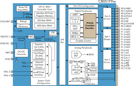
The 'big lever' for controlling power consumption is the supply voltage. Adding on-chip voltage conversion, such as a low drop-out voltage (LDO) regulator integrated on a device such as Silicon Labs' C8051F9xx, can yield significant dynamic power savings by providing a steady 1,8 V supply to the MCU's digital core (see Figure 2).
Benefits of voltage conversion
To illustrate the benefits of using an LDO regulator, it is helpful to restate the CMOS dynamic power relation:
P = C x V² x f = V x (C x V x f) = V x I, where the dynamic current I = C x V x f
It is common to normalise the dynamic current to a frequency of 1 MHz and a particular supply voltage; for example, one popular low-power MCU has a dynamic current consumption of 220 μA per MHz at 1,8 V. Without supply regulation, this metric would increase to (220) x (3,2/1,8) = 391 μA per MHz when the supply voltage is 3,2 V.
With an LDO, the battery current will remain fixed at 220 μA per MHz across the entire supply range. By migrating to a more advanced 0,18 μm CMOS technology, the digital logic would be much faster and would consume 20 to 30% less current. It could easily operate at voltages lower than 1,8 V, but available Flash memory technologies require at least 1,8 V, and many analog peripherals need 1,8 V or higher supplies to fulfil performance and application requirements.
Figure 1 shows that no one- or two-cell configurations result in voltages between 1,6 V and 1,8 V. By choosing an MCU core supply voltage within that window, the supply can be provided by an LDO in two-cell mode and by an inductor-based DC-DC boost converter in one-cell mode. For a given battery configuration, the voltage conversion will always be either down or up over the full lifetime of the battery, avoiding dynamic transitions from one mode to the other. An integrated DC-DC boost converter, such as the one integrated on the C8051F9xx, adds some complexity but provides considerable system cost and size benefits by enabling one-cell operation.
While an LDO has been shown to provide significant power savings in two-cell operation, a DC-DC boost converter can provide even higher overall power efficiency than the LDO. All else being equal, a 1,8 μm, one-cell design using an 80% efficient DC-DC boost converter will consume about half the power of a traditional 0,35 μm, two-cell design without an LDO.
Sleep mode requirements
Achieving maximum energy efficiency (and battery life) translates into making sure that the MCU operation is optimised in the waking and active modes so that the device spends the majority of its time in a very low-power sleep mode. In some applications, the sleep-mode current is the parameter most responsible for the overall energy consumption.
Minimising sleep-mode current requires the LDO and DC-DC converter to be shut off, cutting power to the digital core. They must also turn on very fast to enable the MCU to wake up quickly. Modules that remain functional in sleep mode (such as power management circuits and an RTC) must operate from the unregulated supply range of 0,9 to 3,2 V.
Cutting power to the digital core logic also prevents its off-state leakage from contributing to the sleep-mode current; however, the MCU must preserve RAM contents and the state of all registers during sleep mode, so that code execution can resume right where it left off. It also needs some form of continuous supply voltage monitoring (or 'brownout' detection) to ensure that the state is not corrupted if the supply voltage drops below the minimum retention voltage.
Finally, the MCU should be able to exit sleep mode from either an external trigger event or an internal timer, preferably one that provides both crystal- and RC-oscillator options. To ensure the longest battery life, the typical chip-level sleep-mode current (including a brownout detector and 32,768 kHz crystal oscillator) should be less than 1 μA. For example, the C8051F9xx has a typical ultra-low sleep mode current of 50 nA, including brownout detector, and fast wake-up from sleep mode (2 μs typical in two-cell mode, less than 10 μs typical in one-cell mode).
Minimising the time spent in active mode
While an MCU is transitioning between sleep and active modes, it is in a higher current state but is not doing any useful work. A fast wake-up time saves power and provides quick response to time-sensitive triggering events, such as waking up from serial port activity. Designers should avoid using a slow-starting crystal oscillator for the high-speed system clock; an accurate, quick-starting on-chip oscillator is a better alternative.
The startup behaviour of analog modules can also have a major impact on the amount of time spent in active mode - voltage regulators or references utilising external decoupling capacitors can take milliseconds to settle.
When active, the digital core should operate at its maximum clock frequency, because doing so effectively amortises any static current consumption over more clock cycles to yield a lower 'μA per MHz' metric. This metric is more useful if it includes all sources of static current, such as the supply voltage and clock monitors, reference circuits, LDO and the system clock oscillator.
The advantages of an integrated solution
Using a traditional MCU with an external LDO regulator or DC-DC boost converter cannot match the performance of a fully integrated solution. The integrated device is bound to be significantly smaller and cheaper. The integrated voltage converters will typically have higher efficiency, because they can be tailored to the requirements of the MCU core.
Finally, an external voltage converter cannot be shut off in sleep mode, because the MCU would then lose its supply voltage. Some external DC-DC boost converters have 'standby' modes that can power a sleeping MCU, but the standby mode current is typically in the tens of microamps, measured at the battery.
| Tel: | +27 11 608 0144 |
| Email: | [email protected] |
| www: | www.nuvisionelec.com |
| Articles: | More information and articles about NuVision Electronics |


© Technews Publishing (Pty) Ltd | All Rights Reserved
 printer friendly version