


Over the last few years I have been asked to examine examples of ball grid array (BGA) defects which are referred to as dropped ball.
This type of defect can be found at different stages in the manufacturing process depending on its root cause. It can be difficult to detect even under package optical or X-ray inspection as the separation gap can be extremely small.
First, it is important to define what 'dropped ball' really means in practice: 'Dropped ball – the loss of one or more balls from the base of an area array component and found during inspection of the component or after first or second side reflow.' This seems appropriate as a definition but many people may have a different description. Other literature defines it as 'Balls separating from the package interface during drop testing, vibration, flexure or temperature cycling.' Obviously this is the point of doing environmental testing: to find the weakness of the interconnection or prove the reliability of the joints.
Balls frequently separated from the package in the early years of BGA use during handling and placement. This is less common today due to the control of area array manufacturing processes and the quality control procedures in component assembly lines. Automatic optical inspection is used along with sample shear testing of the ball-to-substrate interface after reflow.
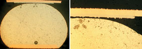
Figure 1 shows the loss of two balls from a BGA. The gold-plated pads are still clearly visible, indicating that the balls were never soldered to the BGA pad. Either lack of flux, poor pad solderability or ball oxidisation could be the root cause of this problem.

Figure 2 shows a section taken of a ball separating from the package; this was found after reflow. Balls separating from the component package during the reflow process, which still show the wetting of solder on the package, means that the solder must have been in a liquid state. Therefore, some force or movement was applied to the solder, allowing it to be snapped from the pad surface. This is more the type of fault that warrants the description 'drop ball'.
Each type of ball drop can generally be illustrated by the way the ball separates from the surface of the package termination pads. In the case of drop testing or shear testing the failure site will have a hard fractured surface on the pad and the ball.
If the balls drop during reflow or rework, the surface of the pad will probably still be perfectly wetted with solder. This would happen if in a liquid state the solder surfaces are stretched and separated. The appearance of the ball or solder will also look different if separated in air or nitrogen environments. Ball drop could also occur and has been seen on BGAs running over a wave soldering system with top side preheat, however the ball may not be round but rather elongated when examined.
During normal reflow, low temperature balls will become liquid and be in a liquid state for a period of time during reflow. As the solder ball is already attached to the package, this will result in a change in the thickness of the intermetallic layer between the alloy of the ball and the nickel. The gold will have gone in to solution during the original ball attachment process. If the solder paste and the ball have the same alloy mixture there will be little to indicate any change. If a different ball alloy is used like tin/silver or tin/silver/copper there would be a difference in the final joint alloy due to the paste that is used. If tin/lead paste is being used this will probably be the most noticeable.
When soldering a BGA to a nickel/gold board, you will see a thinner intermetallic layer at both joint interfaces as nickel is not very soluble in tin. If the surface of the board is copper, silver, tin or solder levelled, you will see evidence of more copper at the interface. Simply put, copper is more soluble in tin, even more so with higher process temperatures and higher tin content solders.
In the case of double sided reflow, the balls could reflow again but this would depend on the setup of the oven profile and the ball metallurgy. Normally if balls reflow on the second side, they only change slightly in shape, unless the board or BGA package warp. If the BGA warps during the first or second reflow operation, you would expect elongated or compressed joints. During wave soldering, the top side of the board should not be allowed to reflow again. BGA terminations can be separated in this way but normally only on the board surface and not the package.
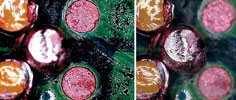
Figure 3 shows the typical pad surface seen after a shear testing experiment on a pad. In this case the surface is fairly flat, indicating that joint separation will have occurred at the nickel pad interface.
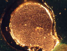
Figure 4 shows the surface of a BGA ball and pad after testing with a dye penetrant indicator. Our test samples show both surfaces are uneven, suggesting a failure in the solder – possibly in the intermetallic.
Area array packages that use solder mask defined pads may exhibit some specific issues during soldering. The solder mask could expand or lift from the surface of the component at elevated temperatures. This could cause the solder ball in a liquid state to become detached from the pad surface like the example in Figure 2. Satisfactory wetting of the package pad would still be present and the ball may still have a rounded shape rather than a rough or brittle surface. The shape of the ball and the surface of the pad would also be dependent on the use of nitrogen in the reflow process.
It is also known that solder mask can outgas during reflow, one of the reasons that printed boards are baked prior to traditional and non-flow underfill. It is possible that this could also occur on a termination with resist-defined pads. As the solder mask increases in thickness more gas could escape, leading to force applied to the liquid solder balls which would of course overhang the aperture of the resist-defined pad. Even if the solder ball on the original component did not overhang the solder mask, which it must do, the increased volume of solder provided by the solder paste would seal the edges.
Resist-defined pads will be more prone to void trapping regardless of the reason for the voids. The thickness of the solder mask will increase their retention. Often when conducting dye and pry tests on BGAs, the author finds a high concentration of voids at the pad interface of the component when there are dimple ball terminations. This type of design has more of a pear-shaped solder ball.
If the suggested reason for separation is correct then gassing from other sources could also lead to ball drop. If voiding were present in the termination from the assembly process, it could rise in the solder ball and end up at the package/pad interface. The thick solder mask and resist-defined pad could exaggerate the problem. Gas has been found on silver finish boards in the past due to incorrect or poor process control in the printed board manufacturing process. The voiding from the surface finish is normally referred to as champagne voiding due to the small size of the voids. This type of voiding is normally only seen at the interface of the printed board pad rather than the BGA package.
Like many defects found in manufacture there can be a variety of causes. The key thing is deciding on possible causes and then finding a way to confirm the cause. If by changing some parameters you eliminate the problem, always go back to your old setup and see the problem resume. Ideally if you can simulate or create the fault again you now have the solution to eliminate it ever happening in the future.
It is important to remember if you are going to conduct failure analysis on problems of this type, that all the process information is provided with the sample. It is also crucial that the board assembly has not been subjected to any other examination prior to review, as this makes the true cause of failure difficult to determine.
For more information visit www.askbobwillis.com


© Technews Publishing (Pty) Ltd | All Rights Reserved
 printer friendly version