


The increasing use of lead-free solder has introduced a new set of process parameters when setting up wave solder equipment for effective soldering. Determining the proper flow characteristics of the solder wave for adequate hole fill is an essential step in achieving a reliable process.
A variety of solder waves exist in the industry, each with advantages and disadvantages when performing lead-free wave soldering. One way to ensure adequate hole-fill is by increasing contact time at the chip wave.
This article presents work done on an innovative way of increasing contact time, hence improving hole fill for relatively challenging board design. This work also examines effects of various process parameters, including nitrogen, on hole fill.
In addition to the experimental work, comparison and discussion of many variations of solder waves including 'A' type waves, laminar waves, dual waves, inerted shrouds, tunnels and non-inerted waves will be discussed. Information will be provided on improved utilisation of old wave solder equipment and the correct selections of new equipment to optimise lead-free wave soldering.
The transition to lead-free wave soldering continues at many sites. As end products become more 'green', process engineers face more complex assemblies requiring the use of lead-free solder. If we think about an SMT assembly line in terms of what is actually manufactured, it leads us to that shown in Figure 1, the solder joint.
Board laminates, components, connectors, etc, are, in general, manufactured elsewhere. This is surprising to some yet when we think about SMT assembly in regards to what is actually manufactured, it leads to the solder joint. Most board assembly companies spend millions of Rands on inspection equipment, placement machines, printing machines and line monitoring, yet invest the minimum possible into the machines that perform the only item that is truly manufactured.
In addition to the complexities of the lead-free wave soldering process, board complexity overall is increasing. Large multilayer server boards are increasing the demands upon the wave solder process, whether it be lead-free or lead based soldering. Though not produced in large volumes, the Rand value and profitability of these high end board assemblies drives the need for high first-pass yield and minimal rework.
When soldered on conventional wave soldering technology, these boards are characterised by low yield, slow production speeds and rework, which increases the latent failure risk. The main process problem experienced is hole fill. Thick substrates, heavy ground planes, and large components rob the heat necessary for a solder joint to properly form. Long contact solder nozzles now exist that can improve the yield, increase the soldering speed, and improve the hole fill for successful soldering of these complex assemblies.
Solder nozzle variations
Wave soldering machine manufacturers provide many nozzle variations and configurations with a plethora of gadgetry and widgets within or surrounding the solder wave, all with claims of unsurpassed soldering performance. With the assumption that the substrates and components are not defective, what is required for good solder joints is plenty of heat, contact time, adequate flux, solderable surfaces and good flow characteristics when the circuit board exits/peels away from the wave.
When troubleshooting wave solder process problems, keeping these basic requirements in mind can go a long way in solving the problem quickly. Nifty nozzle widgets will not yield acceptable soldering if the basic soldering requirements are not up to par.
In the simplest of categorisations, wave soldering is done with either a single wave or a dual wave process. Single wave systems consist of some type of a laminar flow smooth wave, while dual wave systems have an additional wave, preceding the smooth wave, which is turbulent in nature.
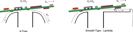
Of the smooth wave systems there are two basic types. The first type is known as an 'A' wave and has a bidirectional flow with high velocity on both sides of the wave. The second type is characterised by a high velocity flow on the leading side of the wave with a slower flow, matched to the conveyor speed, on the trailing side of the nozzle known as the Laminar or Lambda type wave.
Turbulent waves, used in dual wave systems, are generally narrow in width and are... turbulent. These provide additional contact time, reduce the shadowing effect of components, and make extra dross. With the escalating price of lead-free solder, if it is not needed, do not use it. Figure 2 illustrates the basic waveforms provided by wave solder manufacturers.
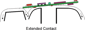
Recent developments have provided for an extended contact dual wave system known as the Dwell Max, whereby a wide turbulent wave is combined with an extended contact smooth wave. This setup is becoming popular for highly complex, thick substrate, palletised server boards and is illustrated in Figure 3.
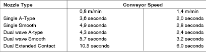
Each nozzle type and configuration will have characteristic solder contact/dwell times at a particular conveyor speed. Generally, single wave A-type nozzles will have the shortest times, with the dual wave extended contact systems having the longest. Table 1 gives contact times for the various common types of nozzle configurations.
Wave soldering atmosphere
Along with the various nozzle configurations that are available, we have the choice to solder in the air atmosphere provided by Mother Nature, or an inert nitrogen environment. Again, all sorts of gizmos and gadgets exist to provide for the 'best' inert atmosphere for soldering, but the choices boil down to two types of systems: boundary layer and tunnel.
Tunnel systems provide an enclosure surrounding the wave solder area of the machine and completely inert the product and solder bath as the substrate passes through. Early tunnel systems inert the entire process including the preheat sections. Experience shows that the extra nitrogen consumption and maintenance required for these systems are excessive. Over time, tunnels that inert in the wave area only have become the preferred system when inerting is required.
Boundary layer systems inert the lower side of the circuit board only and utilise the circuit board itself to provide for the inert atmosphere. Tunnel systems create much less dross, provide for shiny top side solder fillets, and are more expensive to operate in terms of maintenance, nitrogen consumption and capital expenditure. Boundary layer systems create a bit more dross, lower equipment costs and only inert the area where the action is taking place with the solder wave.
Nozzle selection
With all of the options available, which is the best for the lead-free applications? Unfortunately, there is no one system that will satisfy all. Each process owner must review the products that are to be manufactured on an assembly line and choose the type of system that will serve their needs the best.
'A' type waves, with their short contact times, may be completely adequate to solder simple thin lead-free circuit boards but will cause difficulty when soldering products with any complexity or thickness. Extended contact waves may be great for large server boards soldered with lead-free, but may delaminate a thin, lead-free, consumer type product. Good up front board design and process development with the machine manufacturer is strongly recommended before choosing any equipment configuration. Table 2 categorises basic board complexities and can serve as a rule of thumb for wave solder nozzle selection.
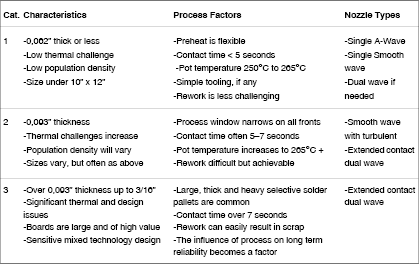
Given the focus of this article, the continued discussion will centre on the multilayer type 3 thick server board and will look at solving the hole fill difficulties when soldering in lead-free.
Boards with hole fill greater than 0,093”
Prior to the development of the extended contact dual wave system, process engineers were limited to slowing the conveyor speed to increase contact time and achieve better yield. Unfortunately, this decreases productivity and increases thermal degradation of the product. To compound the problem, slower speeds in the A-type and smooth wave nozzle systems allow for an increased drop in temperature between the last preheater and the first wave, as well as between the two waves in a dual wave system.
These drops in temperatures needed to be made up and therefore driven at even slower speeds as the entry contact lengths of the solder waves would be reheating the joints and would be lost for the process. Additionally, solidification of the solder joint between waves causes increased degradation of the remaining flux that is above the partially filled solder joint.
The solution was to provide for more contact and to minimise the drop in temperature as the circuit board passes between the two waves. This was solved by significantly increasing the width of the initial turbulent wave and by minimising the gap between the turbulent wave and the smooth wave. Increasing the width of the turbulent portion of the solder wave increases heat transfer over a similar length smooth wave.
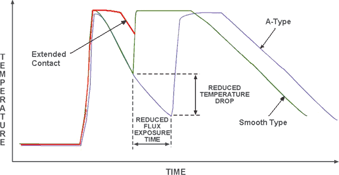
The turbulence and activity of this wave provides a higher conductive heat transfer to the solder joint. These improvements have been very beneficial in achieving higher yield and increased productions. Figure 4 illustrates the solder joint thermal profiles that can be expected for the A-type, smooth and extended contact dual wave systems.
Process testing
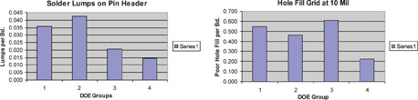
DOE testing was conducted to compare the extended contact dual wave system with the dual smooth wave system. Hole fill, shorts and excess solder (lumps) were recorded for QFPs, through-hole components and ground pins. The test board used was a 0,093” thick board with inner layers of 2 oz. Cu. Coating was OSP and one flux was used for all testing as well as one solder alloy (SAC 305).
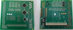
Initial screening tests were completed to determine the low-end deposit rates for the flux that was then used in all testing. Tests were conducted in both air and in a nitrogen tunnel and tests were conducted with conveyor speeds set to provide for both a 3 second and 6 second contact time on the smooth wave. The test vehicle used is shown in Figure 5.
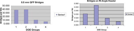
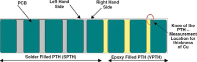
At the conclusion of testing and statistical analysis of the data, the extended contact system performed overall superior to the smooth wave system in both nitrogen and air. Figures 6 and 7 show key gross results. In reference to the figures, the DOE groups are as follows:
1. Extended contact dual wave in air.
2. Dual smooth wave in air.
3. Dual smooth wave in nitrogen.
4. Extended contact dual wave in nitrogen.
Contact time versus copper loss
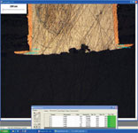
A concern in increasing the contact time is the possibility of degradation of the copper pads and plated through-holes (PTH) due to the dissolution and erosion effects of solder, especially the high tin-content lead-free. An additional DOE test was conducted to analyse this effect. Four factors were established for the DOE: alloy type, conveyor speed, waveform and board vendors.
Board vendor was used as a variable to reduce the sway of data otherwise possible if you used only one board, from one vendor, with one date code. Using two vendors and two boards can confirm that results can translate to a variety of pieces. Response factor was the thickness of Cu from the solder filled plated through-hole. PTH sections were taken and Cu thickness measured and compared between virgin epoxy-filled and solder-filled PTHs.
Alloys used were SAC305 and proprietary tin-copper-nickel alloy lead-free solders. Conveyor speeds used were 1,5, 3,0, and 4,5 ft/min and two board vendors provided substrates. A total of 36 runs were completed. Figure 8 illustrates the method used for determining the before and after thickness changes.
It should be noted that variation in Cu within a board was pronounced and reached as high as 50 microns, however this variability was factored in when comparing the before and after effects. Figure 9 shows a typical cross section of one of the test samples.
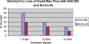
Of the four factors considered, the wave form had the largest effect on Cu erosion. The three wave forms tested were single wide turbulent wave, single smooth wave, and dual waves with both on. Figure 10 shows the measured Cu loss between the two alloy types tested at the three conveyor speeds.
Overall conclusions drawn from this testing were:
1. Copper is removed due to contact time.
2. The Sn-Cu-Ni alloy, as predicted by other work, did remove less material.
3. There was not as strong an indication that erosion was more significant than dissolution.
4. The finding of board and the board vendor variation is significant not only because of the range from hole to hole, but because it should drive a whole different approach to future claims of copper loss strictly due to the alloys used.
5. Long contact solder processes in any alloy will bear influence on knee dimension, and consequently are a consideration in process design. Unfortunately, the quantitative data needed to make a sound process decision require micro-section analysis. Added to this, the variation in the single board, and between boards, much less between different lots and different board vendors, is a completely uncontrolled variable at this time.
Field experience
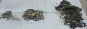
Feedback from users utilising the extended contact dual wave within a tunnel has been positive. At one site, defects were reduced by 47%, improving the defect rates from 47 dpm (defects per million) to 25 dpm. This product was a large thick server type board. Hole fill was improved and solder voids eliminated. Additionally, dross was reduced from 1,4 kg/hr to 30 grams/hour, increasing the de-dross maintenance interval from every 8 hours to 72 hours.
Figure 11 shows a visual comparison of the dross produced between a system running in air (right), boundary type system (middle), and a tunnel system (left).
Conclusions
Many variations exist between wave solder nozzle designs, each providing different advantages and disadvantages. Differences in wave contact time between these systems are varied and are key factors in providing good quality solder joints. Process engineers should consider the product being soldered and select the nozzle system best suited. Lead-free solder continues to create new process challenges in wave soldering.
Thick complex circuit boards with heavy ground planes create very difficult soldering when soldered on standard type nozzles currently available. Utilisation of extended contact type nozzles will overcome these difficulties and provide improved yield, less operating costs and more reliable products.
Copper dissolution and erosion can be a problem on any solder nozzle where extended contact occurs. It is important that this is understood prior to setting up a process. Work done at numerous locations has proven that some L-F alloys, given long contact times, can completely dissolve an annular ring. Copper dissolution may also occur on inner layers, compounding an in-service reliability concern. Board designers should consider this when designing thick circuit boards that require long contact times. Extended contact soldering, in combination with a full inert tunnel, can provide an extremely flexible and low cost method of soldering for lead-free applications as well as traditional Sn/Pb soldering.
| Tel: | +27 11 704 3020 |
| Fax: | +27 83 309 9785 |
| Email: | [email protected] |
| www: | www.testerion.co.za |
| Articles: | More information and articles about Testerion |


© Technews Publishing (Pty) Ltd | All Rights Reserved
 printer friendly version