


Lack of time is often used as an excuse for not going the extra mile. This is unfortunately also the leitmotiv for many small and large electronic manufacturing companies.
As recently as last month I got a call from a Cape Town company wanting to do training but they changed their mind at the last minute because they were suddenly too busy. I do not believe customer satisfaction can be achieved with companies that put time before quality. Sadly though, this is often the case in South Africa.
To meet some companies’ needs, I have even offered to train their staff on Saturdays only. This also runs into trouble because staff are often not paid their dues and refuse to do training on a Saturday unless they get paid overtime. Do companies really need training? After all, they are all getting on with the job, making some money and seem to be doing OK. But are they really?
The problem here is that most companies lack the controls and metrics to evaluate efficiency before and after training. This by itself would also require some company resources – read time and money. It is a vicious circle.
Motorola some time ago made use of the DPMO measure as an indication of defective parts in a manufacturing process for electronics.
DPMO stands for defects per million opportunities. Putting down or mounting a surface mount capacitor for example could give rise to three defects: the component’s body (be it orientation, cracks, polarity etc) and then the two terminals or solder joints.
Depending on the number of components per PCBA (printed circuit board assembly) and the number of boards over a period of time, this figure is comparable worldwide. At one stage Motorola compared various companies around the world. Since this was more than 25 years ago this information has become almost insignificant today.
However, having a peek at the six sigma adepts’ theories, an acceptably low defect figure would translate into approximately 3,4 DPMO. This figure would still be too high for some companies producing for example 1000 PCBs per day with approximately 250 'opportunities' per PCB.
Six sigma really only applies to companies having long and consistent runs of a vested product range. I do not believe there are many here in South Africa where it would be of real benefit. Six sigma is also based on Juran’s Philosophies, meaning that improvement in quality occurs on a project sensitive basis. In other words improvements do not occur everywhere all at once.
Pareto analysis is a tool also used by the six sigma method and measures cumulative errors or defects that occur in the manufacturing and assembly process. See the graph in Figure 1. The blue bars in the graph represent the number of defects of that particular type, while the purple bars represent the cumulative defect count, from left to right.
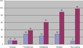
This graph has some of the process criteria listed versus the number of defects of a certain batch of real PCBs produced in 2001, for a GSM payphone manufactured by a local company. You will notice that there is nothing said about dry joints. Why? Because the company in question had long accepted the regular two-year IPC training cycles and all their staff were well informed.
Once again I feel I must repeat myself here for those who do not regularly read Dataweek or do not spend the required time on training: you can find all the legal and commonly used real terms, definitions and even acronyms in IPC’s IPC-T-50G book 'Terms and definitions for Interconnecting and Packaging Electronic Circuits'. This book you will get with my intermediate and advanced training courses or you can order it separately from IPC via www.ipc.org.
You want to know what MBV stands for? Look it up and you will find:
Micro-Blind Via. IMMAU stands for immersion gold, COB is Chip on Board and so on.
Under definitions I would like you to go to the letter D and this I do with good reason. Starting with Dendritic Growth: Metallic filaments that grow between conductors in the presence of condensed moisture and an electric bias (similar to whiskers but not the same).
Dry Glass (Clad Laminate): A general reference to the appearance of a laminate where the reinforcement is highly visible, due to low/lost resin content or poor wetting/encapsulation of the resin to the reinforcement, although the resin coverage is acceptable. Dual Fixture: A test fixture with two separate bed-of-nails units.
What should come between Dry Glass and Dual Fixture? Surely the Dry Joint? Maybe it is under Solder Dry Joint, right? Let us have a look... No, there is no such term mentioned because the dry joint does not exist. The nearest we get is Solder Dissolution: A phenomenon whereby metals (ie, Ag, Au, Cu, Co) are dissolved in the solder. Solder Joint is referred to Solder Connection.
The point is that in my opinion it is better to first get fully acquainted with terms and definitions before we continue with our fancy six sigma, green belts, black belts and master black belt programmes. For fault analysis and proper reporting we could also make use of a component scatter graph to show how the faults are distributed over the area of a particular PCB. Are there defects everywhere? Certain areas only? Concentrated around ICs?
Figure 2 shows an example of a real analysis that took place in 2001 for the GSM pay phone mentioned earlier.
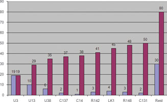
As can be seen from the graph, the Us (IC numbers) contributed to 35% of the defects. Further investigation, visual inspection with microscopes and cross-referencing to the previous graph told us that these ICs had a high number of bridges or so-called shorts. All of the offenders, with no exception, were fine-pitch ICs. Without the proper training, dedication, motivation and test equipment this analysis would not have been possible.
Let us go back now to six sigma and what we can learn from it. One of the implementation strategies of six sigma is the presence and selection of a good 'champion' or team leader. This person is responsible for all of the above steps and the analytical approach to the problem. Motivation and team work are tantamount to success.
The occurrence of unacceptable solder bridges with the fine pitch ICs could further be attributed to a faulty stencil. Too much solder was deposited and resulted in smears or bridges. The champion motivated, pursued and concluded the whole effort and plan.
How does this compare to my MoDePAs approach as discussed in the 23 July 2008 issue of Dataweek? Let us review briefly:
Mo = Motivation. As with six sigma, the champion must be a good leader and people motivator. He or she must also be technically minded and properly trained.
De = Determination. The team must be motivated to go to the end, and determined to find a solution to the problem.
P = Perseverance. A team will often get tired of this daily collection and analysis of data, with all the associated manual plotting and charting. The team leader must push for perseverance and maybe offer some sort of reward.
As = All of this work should result in an after-sales service, with the customer knowing that with this company as a supplier, a guaranteed quality product will always result.
Defects can sometimes be rectified or reworked. It is important here to be conscious of the distinction between rework and repair. Once again if we are not certain, we do not guess but consult our IPC dictionary called IPC-T-50G.
Under Rework we find: (77.1511) The act of reprocessing non complying articles, through the use of or original or alternate equivalent processing, in a manner that assures compliance of the article with applicable drawings or specifications.
Repair-repairing: (77.1502): The act of restoring the functional capability of a defective article in a manner that precludes compliance of the article with applicable drawings or specifications.
Would a de-wetted pad/land be reworkable or must it be repaired? Is de-wetting reworkable in general? If you know the correct answer you may perhaps get away with lesser training. If you don’t know, I suggest you book yourself and your staff for urgent training or re-training.
I shall give you a hint here. Go back to the 25 July 2007 issue of Dataweek. You will get a better idea by reading page 24.
For more information contact Eddy Van den Wijngaerd, +27 (0)21 712 5964, [email protected]


© Technews Publishing (Pty) Ltd | All Rights Reserved
 printer friendly version