


Most RF and microwave calibration practitioners are aware that phase noise can be an important characteristic of signal sources, signal analysers, systems and components. However, they are often not aware of the underlying causes of phase noise, its impact on the performance of equipment and systems, or the significance of phase noise in a variety of calibration tests and applications.
This article presents a broad overview of phase noise, its causes and its impact on modern instrumentation and systems. It also discusses in detail the relevance of phase noise and test equipment phase noise characteristics in the calibration environment – in particular for the selection of calibration standards and performing calibration procedures.
What is phase noise?
An ideal signal source would provide a signal with constant amplitude and frequency. For a sinusoidal signal observed in the frequency domain, its spectrum would be a single infinitely thin line at the relevant frequency. Such an ideal signal may be expressed as V(t) = A·sin(2πf0t) where A = nominal amplitude and f0 = nominal frequency. In practice, real-world signals are disturbed by noise processes and may be expressed as V(t) = [A + a(t)]sin[2πf0t + Δφ(t)] where a(t) represents random variation of the signal amplitude and Δφ(t) represents random variations of the signal phase generally referred to as phase noise.
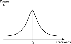
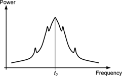
The effect of this Δφ(t) phase noise term is to broaden the signal spectrum, as shown in Figure 1. Another disturbance that often occurs in practice are spurious (deterministic) discrete signals that appear in the signal spectrum as shown in Figure 2, arising from sources such as mixer products, vibration effects, power line frequency, etc. Although their presence may cause undesired effects in the equipment and systems, measurements that consider phase noise alone usually ignore these ‘spurs’.
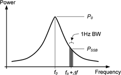
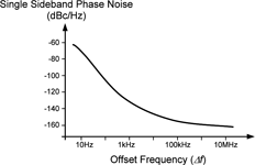
Phase noise is generally expressed as the ratio of the power in one noise sideband (expressed in a 1 Hz bandwidth) to the power at the carrier frequency, derived from the phase noise spectral density – see Figure 3. This is the single sideband (SSB) phase noise generally quoted in equipment and component data sheets, often shown as a plot of phase noise in dBc/Hz against offset frequency (Figure 4).
The associated mathematics is not presented here, but is widely available in other papers and application notes on the subject of phase noise[1,2,3]. Some caution is recommended as these derivations assume the phase variations are small (peak phase variation << 1 radian), and that the amplitude variations (AM noise) are small. If significant AM noise is present, the AM sidebands will interact with the phase noise sidebands and cause asymmetry in the upper and lower noise sideband levels (the AM sidebands have zero phase difference, but the phase noise sidebands have 180° phase difference).
Sources of phase noise
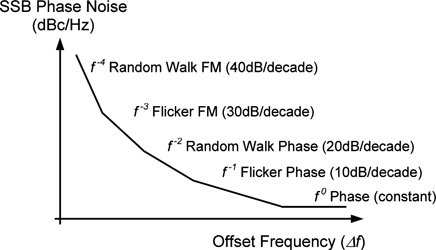
Phase noise is generated in oscillators, from random noise sources such as thermal noise, shot noise and flicker noise, etc. These mechanisms manifest themselves over different offset frequency ranges (Figure 5), and the extent to which they are present depends on the oscillator design and component technology. Often the requirements for low phase noise conflict with those for other oscillator characteristics. For example, widening the frequency pull range of a voltage controlled crystal oscillator (VCXO) will typically worsen its phase noise performance.
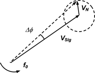
Amplifiers and other active and passive devices can also contribute to phase noise. In Figure 6, the phasor VSig represents the signal voltage, rotating at frequency f0. Noise from amplifiers, active devices, or thermal noise from passive devices is represented by the smaller phasor VN, which causes a change in phase of the resultant signal Δφ, thus adding phase noise as well as amplitude noise.
Equipment and systems generally require signals to be generated at more than one frequency or over a range of frequencies, and employ frequency synthesisers. These synthesisers may simply be one of the many circuit blocks, for example within a communications system, or the main purpose of the device such as a general purpose frequency synthesiser or signal generator. They will typically involve phase locked loops (PLLs), frequency mixing techniques and often more than one oscillator technology.
The overall phase noise performance will depend on the synthesiser architecture, presenting designers with many challenges in meeting the often mutually exclusive requirements of low phase noise together with the other performance criteria. The resulting phase noise performance will generally depend on output (carrier) frequency as well as offset frequency, resulting in the specification tables and performance charts usually found in signal source data sheets.
An appreciation of the reasons why these plots generally have a common overall shape can be gained from considering the simple PLL shown in Figure 7. The corresponding phase noise characteristic is shown in Figure 8. At any particular offset frequency, the phase noise present on the output frequency is the sum of the contributions from the individual circuit elements.
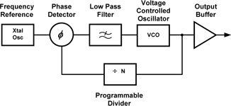
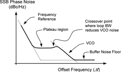
However, one contribution is usually dominant over a certain range of offsets. For example, the frequency reference crystal oscillator dominates at low offsets, and the VCO at higher offsets. A plateau region is typical between these offset ranges, due to the phase detector and the divider (phase noise caused by jitter at the divider input effectively becomes multiplied by its division ratio N). Some peaking in noise level is often observed at the offset frequency corresponding to the loop bandwidth. Above this frequency the loop feedback no longer reduces the VCO noise, adding VCO noise to the plateau level until VCO noise reduces at higher offsets.
At the highest offsets, the noise floor of the output buffer generally dominates. If the output of such a PLL is divided down to produce lower frequencies, the overall phase noise versus offset frequency characteristics are preserved, but the noise is reduced by the division ratio (for example by 6 dB for division by 2).
Phase noise and jitter
The foregoing has treated phase noise as a frequency domain phenomenon, but phase noise on a signal also appears in the time domain as jitter. Jitter is variation in signal timing, and phase noise can be a significant contributor to timing variations.
Impact of phase noise in common applications
Noise of any kind is usually detrimental to the operation of any equipment or system. Examples of the adverse effects of phase noise include:
Radar systems: Doppler radars detect and determine the speed of moving targets by measuring small frequency changes in the returned echo signal. Low-speed targets are affected by phase noise at low offset frequencies and high-speed targets are affected by noise at higher frequency offsets. Airborne radar systems suffer from ‘clutter’ produced by returns from the ground, which are difficult to separate from returns from moving targets, and phase noise in either the transmitter or receiver can aggravate the difficulty. Phase noise at offsets from tens of Hz to tens of MHz is typically significant in radar systems.
Radio communications systems: Phase noise can affect radio communications systems in many ways. Phase noise on the local oscillator used for frequency conversion in a receiver can mask (block) reception of a small wanted signal if it becomes translated in the mixer to fall within the IF (intermediate frequency) passband. Excessive phase noise in a transmitter can cause adjacent channel problems by generating signals in adjacent channels strong enough to mask or interfere with wanted weak signals in the receivers tuned to those adjacent channels. For example, phase noise at offsets from a few hundreds of kHz to around 20 MHz is important for blocking in GSM cellular telephone systems.
Data systems: Phase noise on clock and data signals produces undesirable timing jitter resulting in excessive bit error rates. Modern data systems employ error correction routines, and retransmit corrupted data frames and packets, but with the penalty of reducing system capacity and data rates. Phase noise at offsets from a few kHz to tens or hundreds of MHz is typically significant in high-speed data systems.
Phase noise measurement
A variety of methods are available for phase noise measurement, many of which are complex and best suited to measurement of low phase noise sources. For example, comparison can be made against a low-noise reference (Figure 9). In this case the reference source is locked in quadrature to the UUT source, and the phase noise is demodulated using a double balanced mixer, behaving as a phase detector. The DC output of the low pass filter following the mixer is used to maintain the quadrature lock. A spectrum analyser or FFT analyser is used to measure the mixer output. This method responds to the upper and lower noise sidebands and effectively measures the sum of the two, making the assumption that they are equal when presenting the measurement result. Since it employs a phase discriminator, it does not respond to amplitude noise.
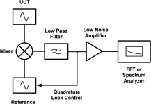
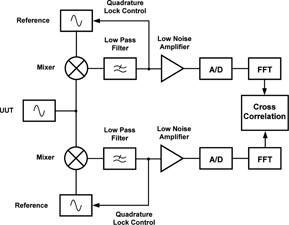
Measurement capability can be improved if a second channel with a separate (uncorrelated phase noise) reference source is used to simultaneously measure the UUT and cross-correlation techniques are implemented.
Commercially available phase noise measurement systems based on the described technique have been available for many years. Some examples use discrete instruments, including low noise general purpose signal generators as the reference. Recent advances in digital signal processing techniques have enabled the use of the cross correlation method within phase noise measurement instruments. Modern solutions include signal source analyser instruments, intended to characterise components such as oscillators, using these techniques to provide state-of-the-art phase noise measurement.
A simpler alternative method is to use a spectrum analyser to directly measure the signal’s phase noise. Modern spectrum analysers include phase noise measurement features, along with the inherent phase noise performance, enabling them to address some of the most demanding phase noise measurement applications.
In the most basic case, the spectrum analyser is set to display the signal spectrum and measure the carrier to sideband ratio at the relevant offset frequency. To obtain the phase noise measurement in dBc it is necessary to apply various normalisations and corrections[4]:
* For the shape of the analyser resolution bandwidth (IF) filter (Gaussian/rectangular) Noise BW = 1,2 x Analyser RBW.
* For the measurement bandwidth, normalising to 1 Hz = 10Log10(Noise BW in Hz).
* For the analyser peak detector average/rms response = typically 1,05 dB.
* For the analyser logarithmic compression of the noise signal peaks = typically 1,45 dB.
For example, if the noise level relative to carrier is -70 dBc when measured with a 1 kHz RBW, the phase noise is -70 -10Log10(1,2 x 1000) + 1,05 + 1,45 = - 98,3 dBc/Hz.
Most modern spectrum analysers include marker or cursor functions which automatically perform these corrections and present a readout of noise level directly in dBc/Hz. Many high-end spectrum analysers also include more sophisticated phase noise measurement features, capable of directly displaying a plot of phase noise versus offset.
Spectrum analyser noise sideband calibration
As phase noise measurement is an important application for spectrum analysers, testing the analyser’s noise sideband performance is a critical part of spectrum analyser calibration. The majority of spectrum analyser calibration procedures verify noise sidebands (phase noise) performance at a single input frequency, usually between 500 MHz and 1 GHz.
Many modern analysers include a phase noise measurement feature, relieving the user of the need to understand and apply the corrections described earlier in this paper to obtain the measurement result in the required dBc/Hz units. Some older analysers specified their noise sidebands performance as sideband suppression in dBc, thus avoiding the need to convert to dBc/Hz. These analysers were popular before phase noise measurement became a widespread spectrum analyser application and often did not have phase noise measurement features.
In principle, the test is easy to perform, but does require an input signal with sufficiently low phase noise to adequately test to the analyser’s specification. Figure 11 shows a typical setup. As analyser manufacturers have improved instrument specifications, their calibration has placed tougher demands on the signal sources used for testing.
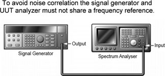
The phase noise measured by the spectrum analyser is a combination of the analyser’s phase noise and that of the signal. Ideally, the contribution of the source will be insignificant, otherwise the measured noise value will be in error. Consequently, phase noise performance becomes an important consideration in selecting a signal source for spectrum analyser calibration.
Signal source selection considerations for spectrum analyser calibration
When selecting a signal source the key issue is “how much better than the UUT should the source phase noise be?” The author has posed this question to many calibration practitioners, with answers including '10 dB', '6 dB', and 'at least 3 dB, but in some cases we tolerate 1:1 because finding low noise sources for testing high performance analysers is difficult and expensive'.
Figure 12 shows how the noise of the source contributes to the measured noise (the x-axis is the difference or margin in dB between the source noise and the UUT noise).
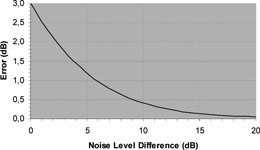
If the source and UUT noise levels are equal (0 dB margin) then the measured noise level is in error by 3 dB (too high). With 3 dB margin, the error is 1,76 dB, and with 6 dB margin the error is 0,97 dB. If the contribution of this error is small, it is usually considered as one of the measurement uncertainty contributions. However, when making noise measurements, low margins approaching 0 dB equivalent to test uncertainty ratios (TURs) approaching 1:1 will not give ‘false acceptance’ of an out-of-tolerance UUT, and may be acceptable in many quality systems – particularly at points not critical for the UUT applications. If the source noise contribution is too large to be considered acceptable in this manner with the test yielding a ‘better than’ result, a lower noise source must be found.
Generally the only information available to assess the signal source noise contribution is the signal source’s specifications, and the actual noise level for the particular source being used is unknown. If the signal source noise level is known at the signal and offset frequency being measured – for example from a calibration report for the signal source which contains phase noise measurement results – a correction for the source noise may be applied.
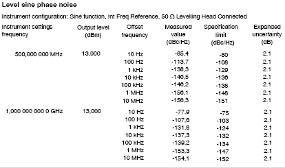
Figure 13 shows an extract from a calibration certificate for the Fluke 9640A-LPN RF reference source, a low phase noise instrument designed for such calibration applications. Measured phase noise data is included to enable users to apply noise corrections if required, or when considering margins to use the actual noise levels, which can be somewhat lower than its published noise specifications.
Identifying and obtaining a source with sufficiently low phase noise throughout the required offset frequency range can be difficult, particularly when testing some of the popular higher performance analysers. Designing a signal generator with low phase noise at all combinations of carrier and offset frequencies can be challenging. A generator design may have good performance at low offsets (close-in) to the detriment of its high offset (far-out) performance and vice-versa. Consequently two signal generators may be required, one to test the analyser low offset performance and another to test the high offset performance.
The 9640A-LPN is optimised to provide a balance between close-in and far-out phase noise performance, eliminating the need for two signal generators. For the most demanding requirements, a simple cost-effective approach is to employ an external filter to provide additional suppression of the signal generator noise sidebands at the offset frequency of interest. For example, a bandpass filter may be used to improve the generator’s high offset phase noise.
The UUT analyser’s own noise floor can also influence the measured noise sideband result. The analyser noise floor performance is described in its displayed average noise level (DANL) specifications, and its DANL performance is usually verified as part of the calibration. As the noise sideband level approaches the DANL floor at the higher offset frequencies the measured noise level becomes increasingly in error. This error can also be determined from Figure 12.
The error can either be considered as one of the measurement uncertainty contributions, or a correction can be made. A correction can be applied to the measured noise sideband level by also measuring the analyser noise floor with the signal source disconnected. The measurement values are converted to linear power units (Watts) and the DANL power is subtracted from the measured noise sideband power. This true sideband power is then expressed as a logarithmic ratio (dBc) and converted to the required dBc/Hz phase noise value.
References
1. Aeroflex Application Note #1: Phase Noise Theory and Measurement.
2. Good Practice Guide to Phase Noise Measurement, Measurement Good Practice Guide No. 68, National Physical Laboratory, Teddington, UK.
3. Hewlett Packard Product Note 11729C-2: Phase Noise Characterisation of Microwave Oscillators.
4. Rhode & Schwarz publication Fundamentals of Spectrum Analysis PW0002.6635.
For more information contact Comtest, +27 (0)11 254 2200, [email protected],za, www.comtest.co.za
| Tel: | +27 10 595 1821 |
| Email: | [email protected] |
| www: | www.comtest.co.za |
| Articles: | More information and articles about Comtest |


© Technews Publishing (Pty) Ltd | All Rights Reserved
 printer friendly version