


The whole point of an FPGA is flexibility. We could also mention integration and say instead that the whole point of an FPGA is flexibility and integration.
But then there are cost savings. So the whole point of an FPGA is flexibility, integration and cost savings. Yet there is also power reduction. And then there is security . . .
All these advantages (and others besides) have made FPGAs very popular over the years. Engineers like the flexibility, space and power reduction and integration that FPGAs provide. So it stands to reason that adding more flexibility, more integration and more cost and space savings would be a good thing. Actel’s new family of SmartFusion chips takes all the traditional advantages of FPGAs and combines them with equally flexible analog circuitry and the world’s most popular embedded processor. It is all rolled up in one package, and all under the user’s control. It is a single ‘super chip’ that could very probably be the only chip in a system, providing inevitable space, time, power and cost savings.
Overview
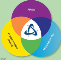
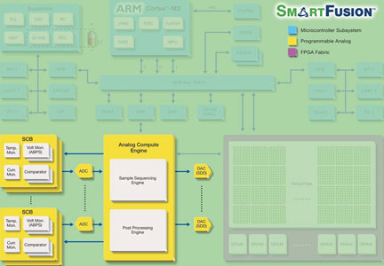
SmartFusion has three basic features: a processor, an FPGA and an analog circuit block. All three are in the same chip and all three are programmable. The processor is programmable (through software); the FPGA is programmable (through normal FPGA design flow); and the analog circuitry is programmable (through some clever configuration software). Almost everything about SmartFusion is under the engineer’s control, so even though the chips themselves are standard when they leave the factory, the products they enable are anything but.
SmartFusion can be thought of as a three-part chip or a three-legged stool that includes the processor, the programmable logic on an FPGA, and the programmable analog circuitry. A typical engineering team will include people who specialise in each domain: software, logic design and analog. All three will be comfortable with SmartFusion, but a single engineer working alone can also use SmartFusion as a universal, all-in-one component to realise almost any design.
All three design tools and domains are integrated, and all three talk to one another. Some designers will see SmartFusion as a processor; some think of it as an FPGA; some consider it an all-purpose analog chip with a processor and FPGA attached. All of that is true, because no one part is more or less important than the others. But what is really interesting is that it brings all these things under one roof. That is not just good for space and cost savings – it also makes designs more secure and more flexible. With most or all of a product’s electronics and interconnects inside the chip instead of outside it, a designer does not have to worry about PC board interconnect, unexpected component changes, interface problems, supply-chain headaches, reverse-engineering, power-on surge current or radio frequency (RF) interference.
The security angle
Security can mean a lot of different things, from safety to reliability, to hacker-proofing and more. Saying a product is secure sounds nice but it is not specific enough. SmartFusion brings different kinds of security to a new product; security that is worth considering. It uses Flash memory, not SRAM, for its entire internal configuration; this has been an Actel hallmark for years. It may sound like a trivial distinction, but it is an important one.
When an SRAM-based FPGA starts up, it is a blank slate, so it has to be retrained on every power cycle by reading from an external ROM. That means that (a) the FPGA will not work for several milliseconds until it has been retrained; and (b) all that training is out in the open. In other words, the precious FPGA configuration stream, which the engineer has spent several months or years developing, is there for anyone with an oscilloscope to see. It is as simple as reading a ROM, and there is no way to prevent it. Duplicating the design is as easy as duplicating the ROM.
In contrast, SmartFusion chips use internal Flash memory that has never exposed to the outside. There is no ROM for disreputable reverse-engineers to read. The configuration data never leaves the chip. There is no way at all to tease it out, not even by ‘decapitating’ the part and using an electron microscope to examine the silicon layers. It is utterly and remorselessly secure. A nice side effect of this is that the chip actually works when it is powered up. In other words, it behaves like most other chips do; the way most engineers assume chips are supposed to work.
That is more than just a mere detail. If the main (and perhaps only) component does not work on power-up, what happens to all of its floating inputs and outputs? How does that disrupt power-on initialisation? What will the other chips do, the ones it is connected to, when their inputs are connected to this brain-dead FPGA that has not been programmed? And what is to prevent someone from yanking various configuration pins during that vulnerable pre-configured state? What happens then? There is something to be said for having an FPGA work all the time, every time, just the way it was designed.
Security part II
There is another whole aspect to security that SmartFusion improves. With an FPGA, processor and analog circuitry all on the same device, nothing ever leaves the chip. That is, all the data transferred from the processor to the FPGA, from the analog circuits to the processor or between the FPGA and the analog area, is all secure. It has never passed across an external bus that anyone can snoop. It has never exposed. That is a terrific boon when transferring a large amount of sensitive data throughout a system (oh, and it is also faster and more power-efficient, by the way – who knew going green could have so many benefits?)
It might not be necessary to encrypt data again. If data transactions are being encrypted merely to prevent them from being exposed to prying eyes, that whole problem goes away once the bus transactions are confined on-chip. If nothing leaves the secure area of the chip, the designer can dispense with the cloak-and-dagger obfuscation and encryption and get on with the real work. The design is more secure, too. With none of its internal workings or interfaces exposed, all hackers see is a literal black box. Nothing about the architecture, structure or partitioning is visible or discernable in any way. They may not even know SmartFusion is being used at all: Actel can private-label a chip with a customer’s own logo and part number.
Reuse
A good rule of engineering is never to design anything twice. Management consultants call this ‘design reuse’. It never seems to be practiced as often as it should, particular wheels often being reinvented from one project to the next. With so much programmable logic on the SmartFusion chips, this could present a real problem. How can all that logic be filled without spending months on the task? And is it not likely that somebody, somewhere has already developed similar bits and pieces? Common features like pulse-width modulation (PWM) and Reed-Solomon encoder should not have to be designed from scratch.
That is where Actel’s DirectCore library of IP comes to the rescue. DirectCore contains more than 50 different IP blocks in its library – and they are all free. There are also independent third-party suppliers of IP blocks ready to plug into a SmartFusion design. The same goes for software, which can often be more time-consuming to develop than hardware. Here again, Actel provides a big library of commonly used middleware, such as TCP/IP stacks, file systems, HTTP, SMTP and plenty of other acronym-heavy bundles of code. And again, it is all free for the taking.
Dependence
The sceptical engineer might think, “I like all this, but it means I would be getting my main (and possibly only) component from a single source. That will expose me to nefarious extortion from an unscrupulous silicon supplier.” To which the more reasonable engineer might reply, “How is that different from what you are doing now?” Typically, most or all components are coming from a single source anyway, and drop-in replacements from another supplier are not commonplace. A disruption in the supply of any one of those components can throw a wrench into production.
Statistically speaking, risk is increased by using multiple components and decreased by reducing component count. Ideally, a design would use just one component from one supplier. Even more ideally, that one component would be programmable and customisable so that a designer is not simply buying the same generic component his competitors are using, which would leave no differentiation and no ‘value added.’ But by using a single component that is programmable and customisable, an engineer gets all the advantages of a low-component-count bill of materials plus the freedom and flexibility to design around it. The best, as they say, of both worlds.
Size and cost
When SmartFusion is referred to as a ‘big component’, this does not mean massive in the physical sense. SmartFusion chips are not large, nor are they expensive. This makes them perfectly suitable for something like a battery charger, small motor controller, PC card gadget, display driver or what have you. Big capabilities and big possibilities do not necessarily mean big price tag. Good things come in small packages.
Processor subsystem
For a lot of engineers, the processor on the SmartFusion device is the best part. Or at least, the most familiar part. That is because SmartFusion chips are all based on the popular ARM Cortex-M3. The ARM Cortex-M3 is among the world’s most popular 32-bit processors, and an ideal basis for a mid-range embedded system.
Some engineers hear the words ‘processor’ and ‘FPGA’ in the same sentence and think, ‘Oh no, not another slow, bulky, configurable processor!’ That is not the case here. This is no build-it-yourself construction set with a user-defined instruction set and no software support. Far from it; this is a factory-stock ARM Cortex-M3 processor core, just like millions of other Cortex M3-based chips in use all around the world. ARM offers the world’s most popular 32-bit processor family.
Contrary to popular belief, Intel does not make 90% of the world’s processors. In reality, it is closer to 2%. In contrast, about five times that many ARM-based chips go out the door every week. The Intel x86 chips may dominate the PC market, but ARM-based processors dominate just about everything else. The advantage of all this popularity is, well, popularity. The more popular the processor, the easier it is to find software, tools and talent for it.
Studies show that most engineers choose their operating system and code development tools first, and then choose a processor to run them on. With a vast array of software, middleware, operating systems, debuggers and hardware and software development tools, ARM processors are the de facto choice for smart developers around the world. It is easy to hire programmers with experience with ARM processors and easy to get good support, software and service for ARM-based chips.
The processor hums along at 100 MHz and will deliver about 125 Dhrystone MIPS. For those not familiar with the Cortex-M3, it is ARM’s mid-range embedded processor, much newer (and faster) than the popular ARM7 but less exotic (or power hungry) than ARM’s Cortex-A8 or -A9 processors. It is a 32-bit RISC processor that is extremely well supported with software development tools.
Unlike a lot of RISC processors, the Cortex-M3 has a hardware multiplier and divider, so these basic math functions do not have to be done in software. The processor also has a memory protection unit (MPU), which is like a streamlined memory management unit (MMU). It is enough to segment and rearrange memory maps to suit a designer’s whims, and to prevent rogue code from damaging memory, but not so complex that one has to deal with page faults and translation lookaside buffers (TLB.)
Naturally, the processor comes with its own memory and other resources. In this case, it has got 16 KB to 64 KB (depending on the specific SmartFusion chip) of high-speed SRAM, which can be used for executing code and storing local variables. It has also got anywhere from 64 KB to 512 KB (again, depending on the chip) of non-volatile Flash memory. Initial accesses to the Flash take from five to seven cycles, depending on the speed of the processor. Obviously, as the clock frequency gets higher the cycle time gets shorter, so even though the number of cycles may increase, the amount of time stays the same.
SRAM accesses always take just one cycle, regardless of processor speed. This no-wait-state memory is fast, and it is divided into two banks so that two masters (the processor and the DMA, for example) can both access it simultaneously. Another clever feature is the SRAM’s ‘bit banding’ region that allows a C compiler to store single-bit Boolean flags in just a single bit of RAM, without using up a whole Byte (or Word). There is an external memory controller if the designer wants to expand beyond the chip’s boundaries.
Rounding out the processor area of the chip is a multitude of peripheral controllers. The set includes a 10/100 Ethernet MAC, two I²C ports, two UARTs, two SPI interfaces, a pair of timers and an 8-channel DMA controller.
This article will be continued in the next edition of Dataweek.
About the author
Jim Turley is the founder of Silicon Insider, a technology-business consulting firm advising chip makers, investors, legal professionals and software companies’ manufacturers in the computer industry. He is the editor of Embedded Technology Journal and was previously the president/CEO of a publicly traded microprocessor firm and senior vice president of another public microprocessor IP company, was editor of the prestigious industry journal Microprocessor Report (a three-time winner of the Computer Press Award), editor-in-chief of Embedded Systems Design magazine, and conference chairman of many annual industry events.


© Technews Publishing (Pty) Ltd | All Rights Reserved
 printer friendly version