


Refer to the 31 March edition of Dataweek for the first part of this article.
FPGA-based processors
FPGA-based processors have a chequered history. Some are terrific; some less so. First of all, there are two kinds of FPGA-based processors: soft and hard. Soft processors are those that use the FPGA’s own programmable logic to build the processor core. That uses up some (perhaps most) of the FPGA’s logic, leaving little left over for other circuitry – which defeats the purpose of using an FPGA in the first place.
More importantly, however, these early soft processors just did not work very well. It turned out that microprocessors just did not map well onto the type of logic and interconnect that FPGAs provide. They do not have the right mixture of registers, MUXes, storage and wiring. The result was that soft PowerPC, MIPS or ARM processors implemented in FPGA logic were slow and an expensive waste of valuable FPGA resources.
Following that initial experiment, the big FPGA companies started over with their own FPGA-compatible processors. These worked much better. Actel created CoreABC, Altera designed Nios and Xilinx developed MicroBlaze. In each case, the processor was designed to suit the FPGA’s available resources, rather than forcing an existing processor into an unwilling FPGA. This second generation of soft processors all use FPGA resources much more efficiently, and deliver modest performance at minimal extra cost.
The other kind of FPGA-based processors are hard processors. These do not use an FPGA’s programmable logic at all, but are really standard processors permanently attached to an FPGA. It is the best of both worlds: the processor gets to run at full speed and the FPGA fabric gets left alone to do what it does best. Neither the processor nor the FPGA fabric is compromised, but instead work together.
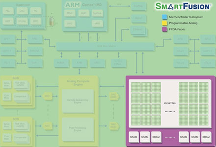
Actel’s SmartFusion family follows this latter philosophy. The FPGA fabric on the chips is entirely free for the user, while the Cortex-M3 processor is well equipped to run at full speed with caches, buses and interfaces suited to its demands.
Analog subsystem
‘Programmable analog’ sounds like an oxymoron, but the concept is elegantly simple and one that will delight both hardened analog engineers and analog-phobic digital designers. SmartFusion’s programmable analog area can be thought of as an FPGA without the lookup tables (LUTs). Instead, it combines the familiar programmable interconnect with an array of analog components and building blocks. By connecting and combining different analog components, a designer can create just about any analog front-end, function or feature they want. There are prescalers, converters, sensors, analog/digital converters, comparators, current monitors, temperature monitors and more.
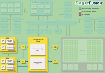
Every SmartFusion has at least one successive-approximation register analog-to-digital converter (SAR ADC). The converter converts voltage into an 8-, 10- or 12-bit number and can do this at 500 to 600 KHz (depending on the resolution). That translates to half a million samples per second, which ought to be enough for most designs. The ADC is fed by a 16-to-1 multiplexer, the idea being that 16 different analog inputs can be sampled simultaneously but the digital value is only going to be read from one at a time.
For conversion in the other direction (that is, digital to analog), SmartFusion has a first-order sigma-delta DAC with effectively 12 bits of resolution. The qualification ‘effectively’ is given because the internal architecture is based on a one-bit DAC, but the noise and resolution performance is comparable to that of a conventional 12-bit DAC. From one to three of these DACs is provided, depending on the specific SmartFusion chip.
The analog portion connects directly to the other two main portions of the chip: the FPGA fabric and the processor’s peripheral bus (APB #2 in the block diagram). This makes good sense, but deserves a little deeper explanation.
The path between the analog circuitry and the FPGA fabric is 32 bits wide, so there is a big pipe between analog and digital logic. This makes the two areas real partners, not just acquaintances in an arm’s-length relationship. Programmable logic can be deeply integrated with programmable analog circuitry, and vice versa. This is much better than having only an 8-bit ‘keyhole’ peek into the analog area, squeezing signals and data through a tiny interface.
The second interface, between the analog and processor realms, also makes good sense. The processor sees the analog block as a peripheral (or several peripherals) so it has no trouble reading and writing values to and from it. From the analog perspective, it sees the processor as a digital source or sink, much like the digital side of a DAC or ADC. In short, it works like one would expect it to.
Where the analog portion of the chip really gets interesting, though, is in its analog computing engine (ACE). It sounds like another oxymoron, but it is actually quite impressive and a big time-saver for programmers and analog engineers alike. In brief, the analog computing engine is like a second processor that can be programmed, allowing the analog circuitry to follow sequences and look after itself without so much processor intervention.
For example, the ACE can automatically adjust the resolution of the ADCs sample by sample, or after a preset amount of time. It could be made to automatically adjust resolution up or down over time, for instance, or delay the samples from one ADC channel to another. The ACE can also launch an analog conversion (either direction: ADC or DAC) based upon a signal coming from the FPGA portion of the chip.
Conversely, the ACE can interrupt the Cortex-M3 processor when some event occurs, such as when a particular sampling level is detected or reached. The ACE can also do its own linear transforms (of the form yy = mx + b, including calibration) or do its own digital low-pass filtering, threshold comparison or state filtering; all of this without intervention by the processor. The CPU can either go to sleep or it can do something else while the analog circuitry looks after itself.
FPGA subsystem
FPGAs are how Actel made its name, and for good reason. All SmartFusion chips include a generous amount of FPGA fabric, starting with 1536 tiles of logic on the smallest A2F060 part. The biggest A2F500 device comes with 11 520 tiles. Each tile is roughly equivalent to a D-flip-flop or three-input LUT.
Summary
Engineering is all about finding the most efficient solution to a given problem. Sometimes a software approach works best; sometimes it is a hardware problem; sometimes the solution lies in the analog domain, and so on. Usually it is a combination of all these things. There is no such thing as a ‘typical’ embedded system because there are so many different engineering approaches to different product requirements.
There is an old saying that when the only tool you have is a hammer, every problem looks like a nail. We have all met inexperienced engineers who try to hammer every problem with the one tool they know, whether it is hardware, software or analog circuitry. But integrating some combination of hardware, software and analog is usually the best and most efficient solution.
Harmonious integration makes for the best engineering solutions, but it also makes good commercial sense, too. Management cuts and reductions in engineering budgets and headcount mean fewer engineers are doing more work. Time and budget pressures certainly haven’t loosened, and product life cycles tend to get shorter, not longer. Nimble flexibility is becoming a corporate requirement, and engineering flexibility can be a career saver. Switch-hitters make great team players.
Any way you look at it, SmartFusion is a powerful three-way combination: whether it is the combination of hardware, software and analog; flexibility, security and cost-effectiveness; or space savings, power savings and time savings.
About the author
Jim Turley is the founder of Silicon Insider, a technology-business consulting firm advising chip makers, investors, legal professionals and software companies’ manufacturers in the computer industry. He is the editor of Embedded Technology Journal and was previously the president/CEO of a publicly traded microprocessor firm and senior vice president of another public microprocessor IP company, was editor of the prestigious industry journal Microprocessor Report (a three-time winner of the Computer Press Award), editor-in-chief of Embedded Systems Design magazine, and conference chairman of many annual industry events.
| Tel: | +27 11 315 8316 |
| Email: | [email protected] |
| www: | www.asic.co.za |
| Articles: | More information and articles about ASIC Design Services |


© Technews Publishing (Pty) Ltd | All Rights Reserved
 printer friendly version