4 August 2010Manufacturing / Production Technology, Hardware & Services
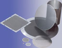
Tech-Etch has a range of MicroEtch screens made from stainless steel, which it manufactures using photoetching technology.
Photoetching enables designers to specify a straight hole or a tapered hole, which facilitates liquid filtration and back flow cleaning. Hole sizes range from 0,076 mm and up.
Unlike stamping, photoetching yields a burr-free product, resulting in cleaner, more efficient screens with greater material integrity. These high-quality screens feature a tighter tolerance on hole sizes and greater dimensional stability than woven wire mesh. This makes them well suited for applications requiring frequent cleaning or in devices where there is mechanical contact. Unlike woven wire mesh screens, the fixed photoetched openings will not change through use.
Typical applications of MicroEtch screens are filters used in the medical market, hydraulic valve screens, fuel filters, laser light filters, extruding screens, as well as particle separation and sizing. Although these screens are primarily produced from stainless steel, other materials are available. Tech-Etch offers a standard line of screens with holes in a 60° or 90° pattern that are available with a maximum guaranteed perforated area of 457 x 533 mm. Other sizes and custom shapes are also available.
FineX: Makes shielding clear Avnet Abacus
Manufacturing / Production Technology, Hardware & Services
Panasonic Industry launches high-transparency, low-resistance, flexible transparent conductive film for electromagnetic wave shield with pre-applied OCA.
Read more...Collaboration is now critical RS South Africa
Manufacturing / Production Technology, Hardware & Services
The message emerging from RS Connect is clear: Organisations can no longer rely on internal optimisation alone to secure performance. Competitive advantage is increasingly being determined by the strength of external relationships, shared capability and coordinated action across value chains.
Read more...Disruption is the new normal. Effortless is the new competitive advantage. Seven Labs Technology
Manufacturing / Production Technology, Hardware & Services
Global supply chains have been under pressure for years. The manufacturers still standing are the ones who stopped waiting for normal to return, and started building something better.
Read more...Clearing the Static: Ensuring effective ESD control Actum
Circuit & System Protection
To maintain reliable electrostatic discharge control, regular testing and accurate measurement are essential, with grounding products and ESD testing equipment being vital.
Read more...World-first 016008 mm component placement
Manufacturing / Production Technology, Hardware & Services
Fuji has achieved the world’s first placement of 016008 mm (0,16 x 0,08 mm or 006 x 003 inches) size components on printed circuit boards with its SMT pick and place machine, NXTR.
Read more...Clearing the Static: The importance of ESD audits Actum
Circuit & System Protection
An ESD audit is the first step in establishing an effective static control programme in the workplace, and will help identify vulnerable areas and potentially hazardous static zones that require improvement.
Read more...Lifecycle and obsolescence: Protecting electronics through process Production Logix
Manufacturing / Production Technology, Hardware & Services
At Production Logix, we believe longevity is not accidental. It is engineered through early visibility, structured response, and disciplined execution, in partnership with our OEM customers.
Read more...Maximising squeegee quality and durability Testerion
Manufacturing / Production Technology, Hardware & Services
Transition Automation has announced two new product advancements designed to improve SMT printing performance and extend squeegee life: laser-enhanced Permalex bonding and integrated edge protectors.
Read more...NeoDen ND2 PCB screen printer ZETECH ONE
Manufacturing / Production Technology, Hardware & Services
The NeoDen ND2 PCB screen printing machine is a fully automatic stencil printer designed to deliver precise and consistent solder paste application in modern SMT production environments.
Read more...Understanding the BGA rework process Techmet
Manufacturing / Production Technology, Hardware & Services
BGA rework is a highly technical process that involves removing the faulty component, preparing the circuit board, and installing a new or repaired device, while maintaining the integrity of the printed circuit board.
While every effort has been made to ensure the accuracy of the information contained herein, the publisher and its agents cannot be held responsible for any errors contained, or any loss incurred as a result. Articles published do not necessarily reflect the views of the publishers. The editor reserves the right to alter or cut copy. Articles submitted are deemed to have been cleared for publication. Advertisements and company contact details are published as provided by the advertiser. Technews Publishing (Pty) Ltd cannot be held responsible for the accuracy or veracity of supplied material.


 printer friendly version