


In spite of all predictions, wave soldering is still alive and well. When the wave is fronted by a high-speed component placer, a high-speed glue deposition machine is also needed. Stencil printing has the potential to be an extremely high-speed process. When coupled with thick stencils, many of the perceived limitations of stencilling are eliminated. These same thick stencils can be adapted to print solder paste in some previously impossible situations.
Why do it?
Nobody in their right mind would want to take a big tub of glue, spread it over a stencil and push it through holes to make glue dots on the board beneath. It is messy, requires a combination of skill and black magic from the operator and then has to be cleaned thoroughly at the end of production. It is so much more convenient to take a fully programmable dispensing machine, drive the head to exactly the right spot, lower it to exactly the right height, turn an Archimedes screw exactly the correct rotation, dispense exactly the correct volume of glue, lift the head and move onto the next site.
Unfortunately, the placement machine down the line is now screaming for a board and you have another 1499 dots to go. The fastest dispenser has an advertised speed of 140 000 dots per hour under test conditions. This is, indeed, fast but it should be noted that ‘test conditions’ generally involve dispensing small dots side by side, densely packed in a small area, thus minimising time between dispenses.
However, stencil printing can be immensely fast. Inline production machines can accept boards of at least 500 x 500 mm and print them in less than 30 seconds. It is quite possible to print 0,6 mm diameter glue dots, spaced at a pitch of 1 mm. Thus, under test conditions, (ie, cheating, with an entire test board covered with such glue dots), more than 30 million dots per hour are easily achieved, should one ever want to. What is more, this includes the board transport time into and out of the machine and the vision alignment process.
Traditional glue printing
Printing machines are used almost universally for applying solder paste to surface mount assemblies, typically some 2000 dots at a time, at a line beat rate of around 12–15 seconds, or half a million solder dots per hour. It is rare for a glued board to have so many dots. Most components need one to five dots of glue, compared with two or three hundred solder dots. However, printing machines are used far less commonly to apply glue. One reason for this is the difficulty in achieving anything but a uniform dot height, thus making it tricky to attach both 0603s and SOICs. If the glue height is optimised for the 0603s, it will not be high enough to touch the underside of the SOICs. Conversely, sufficient glue thickness to hold the SOICs will drown the 0603s, spreading onto the terminations and board lands. Even if there is a simple mix of 0603s and MELFs, the cylindrical shape of the latter requires taller dots than those for the rectangular shape of the former.
Another reason is that traditional stencils cannot be used when boards are already populated with axial and radial components. This is because the leads of these components emerge through to the top side of the board. The stencil would press down onto these leads, thus bending them and damaging the stencil. In addition, the stencil would be held above the board surface, allowing the glue to emerge from the bottom of the stencil apertures in a very uncontrolled manner.
However, there are many occasions when these problems do not arise. The great majority of components are simple chip capacitors and resistors and these can be mounted onto the board as the first operation. Thus the plain, flat board can be presented to the printing machine and the glue stencilled for these components (any additional glue for the remainder of the more awkward components could be dispensed quite quickly). All of the components are placed and the glue is cured, the board is inverted, through hole components are inserted and the assembly is wave soldered.
The stencil used will typically be 0,25 or 0,3 mm thick, with one or two holes per component, some 0,5, 0,6 or 0,8 mm diameter for 0603s, 0805s and 1206s respectively. Alternatively they might be a single rectangular brick of glue having a width of 0,4 or 0,5 mm and a length equal to the component’s length. Round dots have the advantage of looking like dispensed dots, so operators and inspectors are not alarmed by their appearance. However, rectangular blocks tend to stand taller and are even less likely to spread onto the board lands.
On those occasions when both thick and thin glue dots are required, there is a well known cheat that can be employed. The components needing tall glue dots are usually ICs. These are designed so that the component body stands clear of the surface of the board and are always quite large in area and relatively heavy. Thus the glue dots to hold them are also quite large in area. The printing technique can be modified to have two passes of the squeegee assembly. The first is at normal speed and pressure to fill the stencil apertures and press the glue onto the board surface. However, the second is at higher speed or lower pressure, thus leaving a film or thin layer of glue on the stencil surface.
It will be found that this extra glue passes through the large apertures in the stencil but not through the small ones. Thus, normal small dots of glue are printed for the small components but taller dots are printed for the large standoff components. This process is very flexible, the glue height being controlled by adjusting speed or pressure. This can also be a process weakness in that the machine operator can change the glue height by adjusting speed or pressure . . . but are operators to be trusted?
A more controlled method of varying dot heights
When printing solder paste for surface mount applications, there is a well known rule of thumb concerning paste release from stencils. Given a stencil of thickness T having a long, thin aperture cut into it of width W (and length L, but who cares at the moment?), the rule is that W/T should be greater than 1,5, otherwise not all of the paste will release from the aperture. This is a special case of the more general rule of thumb that complete paste release will occur only if LW/2(L+W)T>0,66. In other words, the area of paste sticking to the board, divided by the area of paste sticking to the walls of the stencil should be greater than 0,66.
In actual practice, no matter how large or how small the apertures are, some paste will stick to the walls and some will stick to the board. If the rules are obeyed, an adequate volume of paste will stick to the board. But what happens if the rules are deliberately flouted? Much paste will remain in the apertures and only some will be deposited. Thus if the stencil is made much thicker than is normal (0,1 to 0,15 mm) for solder paste printing and the apertures remain relatively small, little paste will be deposited. Make the apertures progressively bigger and more and more (taller and taller) paste will come out.
This applies similarly to glue printing. Thus by making increasingly large apertures, increasingly tall dots can be produced. As tall dots are needed only for large components, and as all small components have little or no standoff, small, low dots and large, tall dots are produced automatically. What could be better? The dot heights produced are controlled by the glue characteristics and the stencil dimensions, not by the printer operator.
Thick, plastic stencils
It is convenient to use plastic rather than metal sheets when making thick stencils. For example, stainless steel is more than five times as heavy as the plastics used for stencils. In addition, it is difficult to produce small holes in thick metal by laser cutting or etching. Drilling is possible but relatively slow. While both laser cutting and etching plastic are tricky, drilling is much more straightforward.
Machines of the type used to drill PWBs are suitable for this application, as are the drill bits themselves. These are available in a range of diameters that extends beyond what is needed for glue dots. The translation of code from designing boards to programming drilling machines is routine, and drilling produces round holes. These in turn will produce the round dots of glue that operators expect to see. It is convenient to choose a sheet thickness in the range of 0,5 to 1,5 mm as this meets the requirements of material availability, strength, stability and ability to make sufficiently tall dots.
Plastic stencil design
Test stencils have been produced containing a range of hole diameters and various commonly used surface mount glues have been printed through them[1]. Briefly, many glues print to form relatively high dots, while a very few tend to slump. Experience shows that the dot heights produced (up to the thickness of the stencil) vary only slightly with stencil thickness, thinner stencils giving marginally greater height.
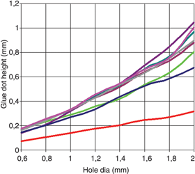
Given one of the many suitable glues, it is straightforward to choose a hole diameter that will give a fair dot diameter and height for a given component. However, conditions and expectations vary from user to user and it is difficult to guarantee that the dot will be optimised. As examples, room temperature, line beat rate, glue type, PWB land layout and the presence of tracks between lands will affect the dot characteristics (the same is true of solder paste printing, hence the frequent wiping of the underside of the stencil).
Glue, being inherently sticky, tends to smear when wiped, so this process ‘correction’ is hardly suitable. It is much better to gain some initial experience, then redesign the stencil to give perfection. Once these optimum dimensions have been derived, they can then be transferred reasonably certainly onto subsequent products – this same philosophy works equally well with normal solder paste stencils and saves much unnecessary stencil wiping. Typical starting points for glue dot dimensions would be some 0,6, 0,8 and 1,0 mm diameter for 0603s, 0805s and 1206s respectively; 1,6 mm for MELFs; two or three dots of 1,5 to 2 mm diameter for SOICs; and five dots of 2 mm diameter for QFPs.
Preinserted component leads
While standard plastic stencils are manufactured from material typically 1 mm thick, greater thicknesses are available. This permits pockets to be machined in the underside of the stencil of sufficient depth to clear the protruding leads of inserted components. This is similar to etching the underside of a metal mask intended to print solder paste onto a PWB that has already been printed with flux or silver epoxy for a flip chip, but on a grander scale. The underside machining can take the form of a large rectangle to clear many leads, a single circle to clear all of the possible positions of an individual lead or a small channel, perfectly aligned to clear an individual lead whose cut and clinched direction is accurately known.
Much depends on the layout of the PWB, its component density and complexity and the state of repair and calibration of the insertion machine. Typically, a stencil of 3 mm thickness is suitable for the components that are found in normal PWBs. The starting point for aperture sizes will be the same used in the 1 mm stencils. Underside routing in all its forms needs a clearance from fully drilled holes of only some 0,2 to 0,25 mm, so dots can be printed easily between inserted component leads.
Printing difficulties
As the stencil thickness increases, it becomes more difficult to force glue into very small diameter apertures (Bernoulli had something technical to say about this). It generally takes a few dummy squeegee passes to pump glue into the apertures of 1 mm stencils (but once full, it takes only single squeegee passes to keep them full). However, it can take tens of passes to fill small holes in 3 mm stencils.
One way to overcome this difficulty is to replace the squeegees with a suitable closed head printing system in which paste pressure is generated independently of print speed. Alternatively (or in addition), the top of the small apertures can be counter-bored, thus reducing the length of the narrow section. Typically, holes of diameter less than 1 mm need such treatment. Whilst helping to solve one problem, it can introduce a second if squeegees are used. The squeegee forces glue into the counter-bore with some ease. However, as the squeegee tip crosses the counter-bore, an increasingly large hole opens up behind the squeegee. The glue tends, therefore, to re-emerge through the top of the stencil rather than being forced down into the small hole.
The closed head systems do not show this effect, of course. One solution when using squeegees is to choose a profile that has a reasonably wide flat formed where the squeegee tip would be (imagine a very worn squeegee). The flat seals the top of the counter-bore and forces glue down into the small diameter hole.
In conclusion, the glue printing process is well established in the surface mount industry and printing through thick plastic stencils has been used in volume production for several years.
Solder paste applications
In the early days of printing glue through thick plastic stencils, some ‘let us see if it works’ trials had also been made with solder paste. Briefly, it did not. The paste could be persuaded neither to go through the small holes nor adhere to the PWB. In addition, there was no obvious application.
Thin metal stencils are used to deposit solder paste onto boards for SMD assembly and, increasingly, to simultaneously fill drilled holes in boards. Thus SMDs are placed on the paste, leaded components are inserted into the paste and all of the joints are formed in the reflow operation. This technique is known as ‘pin in paste’ or ‘intrusive reflow’ and is especially useful on those PWBs that contain many SMDs, plus one or two inserted components such as connectors. It works well on flat boards and eliminates the need for an additional wave soldering process.
However, applications arise when the components are already inserted before the board comes to the printer. Could thick plastic stencils be adapted to print solder paste, not only for regular SMDs but also around the inserted wires? If so, wave soldering would be eliminated by this ‘extrusive reflow’ process. Equally briefly, it could. To date, four styles of manufacture have been attempted and these will now be described.
‘Paste around wires’ or ‘extrusive reflow’
This application was exactly as suggested above. The PWB was panellised as 16 pieces, each being populated with SMDs and inserted components. The SMDs included 0603s, 0805s, 1206s, MELFs, miniMELFs, tantalum capacitors, SOT23s and SOICs. The inserted components were mainly electrolytic capacitors. The 16 piece arrangement made it ideal as a test pattern.
The PWB was for a low-cost consumer application and had been designed for wave soldering. There was little solder resist and no well defined lands for the components, but it was a requirement that all exposed copper should be covered with solder. Hence, in addition to the component solder apertures, a variety of artistic arrangements of holes was provided to cover the bare copper. A stencil was designed at 3 mm thickness so that the inserted leads could be cleared.
Apertures were drilled for the SMDs from 0,6 to 1,3 mm in diameter and those for the inserted components from 2,4 to 3,8 mm in diameter. Initial trials were made onto PWBs pre-populated with the inserted components and again using normal printing grade solder paste. The whole range of possible printing parameters was sampled, varying pressure, speed, separation speed, print gap and numbers of print strokes, but no prints were achieved that were remotely acceptable. It was possible to print small deposits once or twice but after this, no paste would flow through the stencil. The apertures’ length/diameter aspect ratios were much higher than is normal for solder paste printing. They were therefore much more like tubes than stencil apertures.
Hence, it was decided to trial a grade of paste designed for dispensing rather than printing. The results were very much improved so that near adequate volumes of paste were deposited at some of the sites. The paste was removed from the stencil, diluted with IPA in an attempt to increase the flow and more prints were made, with further improved results. It was decided therefore to investigate a range of dispensing grade pastes brought along by one understanding paste manufacturer.
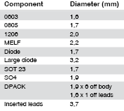
Parts were printed with these materials, using a range of printer parameters, and SMDs were placed on those areas of the PWBs that showed any promise. The samples were reflowed and inspected. The best paste was selected and the few acceptable design areas were identified on a component by component basis. The stencil was redesigned based around these results and the test repeated. This time the SMD apertures ranged from 0,7 to 1,7 mm diameter and those for the inserted components from 3,2 to 3,8 mm diameter. Further artistic arrangements of holes were produced for the bare copper areas.
The best paste and printer settings obtained in the previous trial were used and again anything showing promise was assembled and reflowed. It became clear that the open expanses of bare copper were very difficult to print and tin fully. In addition, there were difficulties caused by the component lands not being designed for surface mount. Lands at opposite ends of components were not necessarily the same shape and size and were sometimes commoned to lands of other components. Thus there were many opportunities for components to move and tombstone. A batch of PWBs was produced with a modified solder resist layer so that lands at least in the spirit of IPC SM 782 were defined by resist. These were printed, placed and reflowed with much more success. Further inspection allowed the final designs to be chosen. Thus the final production stencil had the aperture dimensions as shown in Table 1.
This product ran in volume production and the aperture designs were later transferred successfully to two similar assemblies.
Component rework
A contract manufacturer had assembled a large quantity of PWBs when, unfortunately, a design incident occurred, necessitating the replacement of several components on each panel. These included 0603s and 0,5 and 0,4 mm pitch QFPs. In addition, RF shields had to be removed in order to access the components, and then be replaced. The large number of good components remaining on the PWBs meant that normal printing was not possible and the obvious methods of applying paste by hand or machine dispensing were slow.
This seemed to be an interesting opportunity to play once more with thick plastic stencils. In principal, the stencil could be machined on the underside to accommodate the components that remained on the PWB. In order to clear these components, the stencil had to be 5 mm thick. The faulty components were removed from a quantity of PWBs and a stencil was designed to apply solder paste to the rework sites. Dimensions for the 0603s seemed quite straightforward but the QFPs were a new challenge. In addition, solder paste was required to reattach the RF shields. A quantity of old solder remained on all of the lands, so the printed paste acted merely as a top up and as a source of flux for the reflow.
With no relevant design experience for the QFPs, the first layout comprised a test stencil. Each QFP was divided into four and different hole diameters were used for each quadrant. These ranged from 0,3 to 0,6 mm diameter and so were spanning to adjacent lands at the larger dimensions. The only obvious way to fit the holes into the limited space was to stagger them, alternating between the inner and outer ends of adjacent lands. Test prints were made again using the dispensing grade solder paste but no good results were obtained.
While the deposits for the chip components and RF shields were acceptable, there was no combination of apertures and machine settings that gave consistent paste deposits on the QFPs. The small aperture dimensions were clearly one of the causes. However, the curvature of the tinning on the land surfaces was also a major contributor to the failure. When repeating this on the actual lands, the curvature sometimes broke the gasket between the land and the stencil, thus allowing the paste to bleed. Conversely, the varying area of tinning in contact with the paste in the bottoms of the apertures caused more, or less, paste to be drawn from the apertures. Thus the process remained promising but out of control. The present extrusive process is acceptable for components down to SOICs but not for QFPs.
3D assemblies
A mobile phone accessory manufacturer had a potentially very useful product, if only he could assemble it. Each PWB was some 50 x 30 mm in dimension but it was surrounded by walls some 7 mm high and had components that were within 3 mm of the inside edge of the wall. It would have been easy to dispense paste onto the component lands but with unacceptable time penalties. In addition, the production plan was to have the assemblies palletised as a 4 x 4 array, thus making printing even more attractive.
The components were chiefly SOICs and 0805s and so there was some potential for success. However, with surrounding walls so high, it was clear that an unusually thick stencil would be required and 8 mm was chosen. It was thought that this might influence the paste transfer through the stencil, so a test pattern was constructed. The optimum dimensions from the previous products were used as centre points and these were increased and decreased a little on other units. The holes emerging through the top side of the stencil were deeply counter-bored to reduce restrictions on paste flow down long, thin tubes. In addition, the underside of the stencil was heavily routed, not only to clear the package walls but also the areas of the pallet that surrounded the packages.
The first print trials took place in the customer’s facility, where stencil, parts, pallet and paste came together for the first time. Obvious errors came immediately to light (the stencil had been made for the wrong machine size, the customer had revised the pallet design but not told us …) but these were soon corrected. The trial used squeegees, and a dispensing grade of solder paste that had been provided by the customer’s regular paste supplier.
The results were very poor. It took many squeegee passes to force paste through the larger apertures and life was too short to continue trying to fill the smaller ones. The holes were, therefore, filled by hand, using a pallet knife at a very shallow angle to ‘plaster’ the paste into them. The following few prints showed limited promise but the paste flow rapidly deteriorated. The paste was removed and diluted experimentally using IPA until it resembled the previously successful paste more closely. It was returned to the cleaned stencil and there was some temporary improvement to the deposits. However, the results were far from satisfactory.
The dilute paste was removed and sent to the paste supplier to form a basis for improvement. However, the supplier declined to cooperate. The stencil and parts were carried back to the UK for further trials and these were performed with the known good paste. In addition, the squeegees were replaced by a closed head system that was able to apply pressure directly onto the paste, rather than use the indirect pressure created by squeegees. Results were dramatically improved. The aperture filling took only a couple of passes of the head and the paste flowed onto the lands in its customary manner.
A further trial was set up in the customer’s facility, using the closed head system and the successful solder paste, this time with excellent results. Components were placed in those modules which had promising deposits and were then reflowed and inspected. The optimum aperture dimensions were then chosen and a production stencil was produced.
Interestingly, the optimum dimensions did not always match those of previous products. One possible reason was that the stencil was much thicker, so paste flow was probably more restricted. A second was that, although the component types had been used previously, the present lands did not match IPC SM 782, generally being rather smaller. In addition, there was no solder mask layer, so that tracks leading from the lands tended to starve the joints. Full assemblies were completed and fully tested.
Flex circuit assembly
This final example returned to the original application of printing solder around preinserted leaded devices but added the minor complexity of flex circuits. There had been thoughts originally to use regular surface mount techniques to assemble 0603s on the first side, then use intrusive reflow for the inserted components and the remaining fine pitch device on the second side. However, the thin structure caused the inserted device to sit rather randomly on the flex and the body shape made it difficult to supply sufficient overprinted paste to form sound joints. Extrusive reflow was therefore chosen.
Side 1 was relatively straightforward, requiring the printing, placement and reflow of some small 0,5 mm pitch devices. This was achieved in the normal manner using a laser cut stainless steel stencil that was 0,125 mm thick. As this was part of the overall development exercise, a test stencil was made that incorporated four different versions of the pattern. At one edge of the stencil the aperture width was at a normal ‘best guess’ of 0,250 mm. Rotated 90 degrees and along the next edge was a set with apertures reduced to 0,225 mm.
Similarly on side 3, the apertures were reduced to 0,200 mm width. Finally, on side 4, the apertures were increased to 0.275 mm, just in case most previous experience proved to be invalid. Thus, in one fabrication, and at no extra cost, it was very simple to test print the stencil, then rotate it if necessary to find the optimum dimensions that would allow continuous production with no stencil wiping.
After printing, the parts were taken to a dispenser and glue dots were deposited onto the flex (this could have been done equally well with a printer but would have required buying a second machine or having a large buffered stock of pasted flexes). The 0,5 mm pitch devices were place into the solder and the leaded components were inserted through the flex, the bodies being pressed into the dispensed glue. During reflow, the glue was cured, thus holding the inserted components mechanically.
The assemblies were flipped and presented again to the printing machine, this time fitted with the thick plastic stencil. The pattern comprised deposits over the inserted leads, plus small dots for the array of 0603 components that required attachment. The inserted leads required sufficient paste to form both the connection in the thickness of the flex and the fillets on the top side. The leads extended a shorter distance above the flex than had the previous samples, so a stencil thickness of 3 mm was sufficient. Naturally a test pattern was produced, based on previous good experience. Test prints were made, using the known good paste and a closed head print system.
Excellent prints could be made with the machine running up to its maximum print speed of 150 mm/s and components were placed into these and reflowed. After inspection, certain aperture dimensions were selected as being near optimum. These were used to make a second stencil. This had one image along each side of the stencil, incorporating small variations in aperture dimensions for all devices, and in pitch for the 0603s. There had been fears that the smallest holes that would reliably deposit paste would be too big for these 0603s. Hence these were separated rather widely to eliminate any paste spread under the components that might lead to mid chip solder balls. Test assemblies were made with good success and the optimum aperture dimension combination was selected.
Conclusions
There are a number of ways to print glue for bottom side chip attach successfully and design suggestions are available. These techniques offer very high dot deposition rates that are invaluable when coupled with a high-speed chip shooter.
Techniques are available that allow different glue dot heights to be produced from a single, relatively thick plastic stencil. The heights are controlled by the dimensions of the stencil, not by the ability of the print machine operator.
These stencils are sufficiently thick to include machining on their undersides, allowing the stencil to bridge over, and deposit glue between preinserted component leads. Thus PWB assemblers are free to insert components before or after SMD placement and retain the speed advantages of printing, rather than dispensing glue.
In addition, similar stencils can be used to print solder paste. Their unusual thickness enables them to be used on very non-planar assemblies. Examples of such assemblies have been given, together with design suggestions. Such assemblies include those requiring paste to be printed around preinserted leaded components and into the bases of boxlike packages.
References
[1] 'Plastic stencils for bottom side chip attach', Whitmore, MacKay, Hobby.
Proceedings Nepcon West 1997.
| Tel: | +27 11 609 1244 |
| Email: | [email protected] |
| www: | www.zetech.co.za |
| Articles: | More information and articles about ZETECH ONE |


© Technews Publishing (Pty) Ltd | All Rights Reserved
 printer friendly version