


Jitter spectrum and phase noise on data signals
The previous discussion involved jitter analysis of clock signals. However, the problem to be solved is to understand the root cause of jitter found on a 2,5 Gbps data signal. The time domain representation of a jitter-free data stream is intuitively simple; the frequency domain representation is more complicated. If the data sequence is a repeating pattern, there will be line spectra separated by the pattern repetition rate. The diverse pattern of ones and zeroes with a large variety of times between data edges leads to the line spectra in the frequency domain that follow a sin (x)/x envelope, with spectral nulls at the data rate and its harmonics (NRZ data). For data from a repeating pattern/sequence, the spacing between the line spectra is the pattern repetition frequency.
If a transmitter is timed by a jittery clock, the clock jitter can be transposed on the data stream. In the time domain, the edges of the data will be misplaced from their ideal time positions just as they are for the clock. This is easy to observe and interpret in the time domain, but difficult to interpret in the frequency domain. Random jitter causes the energy of each spectral line to spread. Jitter transfers power from each spectral line into modulation sidebands. Unless the data pattern is very short, or the bandwidth of the modulation is very narrow, the spectrum due to jitter at one spectral line will overlap with the adjacent lines, making jitter virtually impossible to accurately quantify.
This complicated ‘overlapping’ spectrum makes it impossible to derive the jitter or phase noise spectrum of a data stream using a spectrum analyser based test system. However, the jitter or phase noise spectrum of a data signal can be observed using a hardware clock recovery system and monitoring the error signal output from the phase detector. This architecture has two distinct advantages over a spectrum analyser based instrument.
Since the phase detector in this system is designed to sense the phase difference between the recovered clock and the input signal, the measurement is not limited to clock signals but can also include a data signal. In this case the jitter spectrum is equivalent to that of the equivalent clock for the data signal being measured. Also, clock recovery circuits typically have wide-bandwidth analog PLLs capable of tracking or tolerating large wander and modulation typically found in clock signals for personal computer busses, such as with SSC. The internal jitter transfer characteristics of the closed-loop clock recovery system are known, which allows the Fourier transform of the loop error signal to accurately yield the total jitter on the input signal.
Figure 5 shows the jitter spectrum for the PCI Express data signal originally measured and shown in Figure 2. The horizontal axis is logarithmic and is the frequency range of the measurement. The vertical axis is also logarithmic with units of seconds.
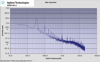
The most dramatic element of the plot is the wide spectral component at 33 kHz. This is the spread-spectrum clocking (SSC) used to mitigate electromagnetic interference problems. In addition to the SSC there are many distinct spectral components which are observed as lines or spikes in the spectral display. The SSC is not a sinusoidal jitter mechanism, but rather causes the signal to deviate according to a triangle function. Thus there are spectral components at harmonics of 33 kHz (3X: 100 kHz, 5X: 165 kHz, 7X: 231 kHz and so on). For a triangle form of modulation the harmonic signals should roll off at a 60 dB per decade rate.
SSC is an intentional or expected jitter mechanism. There are other elements of the jitter spectrum that are causes of undesired jitter. After the SSC harmonics have trailed off (they become insignificant and approach the spectral noise floor a little below 1 MHz) there is a significant spectral component of PJ at approximately 1 MHz. There are also harmonics of the ~1 MHz rate. As discussed earlier, random jitter is seen as the continuous spreading of the signal spectrum. If the line spectra (33 kHz, 1 MHz and harmonics) were removed, the remaining energy is a display of the spectrum of the RJ. The RJ and high frequency PJ are undesirable. Finding their root causes and reducing them will be the key to improving the quality of the 2,5 Gbps signal.
At this point it is useful to measure the 100 MHz reference clock that is used to synchronise the 2,5 GHz data signal. If there is jitter on the reference clock, is it safe to assume that it will directly transfer to the transmitter? After all, carefully designing the loop bandwidths of the PLLs in the transmitter circuitry can clean up jitter from the reference clock. Good engineers know when to make assumptions and when to verify. In this case, verification is easy.
The jitter spectrum for the reference clock (Figure 6) is very similar to that of the 2,5 Gbps data signal. The SSC and its harmonics are the same. The tones at 1, 2, 3. . . MHz are also present. It is clear that the periodic jitter of the data signal is a direct result of the periodic jitter transferred from the reference clock. The spectral noise has a similar shape for both data and clock, except over the 3 to 20 MHz range. The differences may be due to the VCO of the transmitter PLL contributing some random jitter, and the bandwidth of the transmitter PLL altering the spectrum of the random jitter contributed by the reference clock.
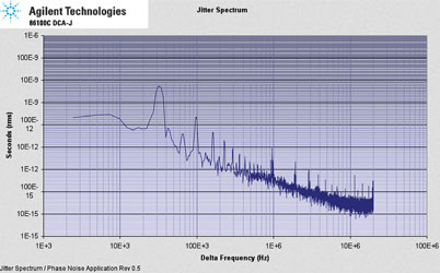
At this point it is worthwhile to take a step back and look at what has been learned. Comparing the jitter spectrum of the data and the reference clock is like a detective comparing fingerprints or signatures. In this case, the ‘jitter fingerprint’ of the reference clock is ‘all over’ the transmitter data. The two jitter spectrum plots look almost identical. Consider trying to make that same comparison with only a time domain representation of the jitter. The magnitude of the RJ and PJ can be gauged, but there is no distinct fingerprint to observe like there is with the jitter spectrum.
There are two approaches to reducing the jitter on the data transmitter. Obviously, improving the performance of the reference clock should directly improve the transmitter performance. Reducing the RJ is a matter of basic oscillator design, beyond the scope of this article. The 1 MHz PJ turns out to be an artefact of how the SSC was generated, and could also be reduced through design. The transmitter jitter can also be improved by designing the PLL bandwidths of the clock multiplier circuitry to clean up the clock jitter. This design process is obviously aided by knowing the spectral characteristics of the clock jitter.
| Tel: | +27 12 678 9200 |
| Email: | [email protected] |
| www: | www.concilium.co.za |
| Articles: | More information and articles about Concilium Technologies |


© Technews Publishing (Pty) Ltd | All Rights Reserved
 printer friendly version