


PCBs are destined for a rigorous life. When they are incorporated into whatever appliance or machine they were designed for, they have to survive several passes through ovens operating at 260°C. In the field they may also be expected to operate in high heat, high humidity and high vibration environments where imperfections could easily develop into fatal faults.
This article delves into the quality control measures employed at Cirtech Electronics’ PCB manufacturing facility.
A delicate process
Printed circuit boards are constructed in fine layers, laid down by chemical and electrical processes onto very thin layers of substrate. Tolerances and measurements are calculated in microns. Producing the high quality PCBs that Cirtech is known for, can only be achieved with the best equipment and chemical processes combined with best practice and rigorous quality control. Whilst PCB fabrication is a delicate process on the one hand, on the other, the boards are subject to high pressure and heat when they are sandwiched into their multilayer formation and to mechanical stress in the drilling and scoring processes.
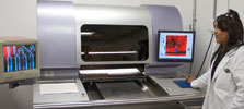
During manufacture, each layer of a multilayer PCB undergoes an automatic optical inspection (AOI) before lamination takes place. This is the only time that the finished tracks are accessible for inspection. Once the layers are laminated, the tracks are effectively entombed. Completed boards are fully electrically tested on the flying probe machine which ensures that the PCB’s circuitry will function as it was designed to.

Why microsections are essential
Although AOI and flying probe tests may give a clean bill of health, there are more potential pitfalls in PCB manufacture than can be detected by the naked eye or the infinitely accurate prodding of electronic probes. The mechanical and thermal stresses that lamination, drilling and scoring exert on the boards can give rise to microscopic faults if they are not executed with care. To complicate matters, these defects occur inside the board and involve the substrate bonding, the through-hole plating and the copper layers that form the tracks.
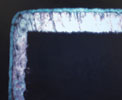
Holes, or vias, are the most critical parts of a PCB. They connect the components on the surface of the board to the circuitry inside the board and thus to each other. Any defect in the via, the through-hole plating, the substrate or the copper of the circuitry will result in circuit failure. The vast majority of vias are drilled with a steel bit, as opposed to a laser or a punch. If the drills are slightly blunt, are run too fast or are left in contact with the board for too long, mechanical and thermal stress is escalated beyond the tolerance of the materials involved and defects will arise.
Many of these defects would only become apparent once the PCB was on the client’s production line or after market, where they would manifest as product failure. The only way to detect faults hiding within the laminations is to sacrifice sample boards. Sections are carefully cut from these boards and captured in resin: this begins the microsection process.
The ultimate quality control tool
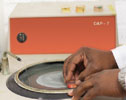
The resin forms a supporting matrix for the sample and prevents any tearing or splitting of the laminations or peeling away of through-hole plating. Once the microsection is captured, excess resin and unwanted PCB material is ground away until the cross section that needs to be examined is exposed. This is usually across a line of vias, so that the edges of the bores, the through-hole plating and the supporting substrate can be examined.
The grinding is done on a wheel. The excess resin is removed with emery paper, lubricated with water. As the required cross-section is reached, paper with progressively finer grit is used. To finish with a scratch-free, optically correct surface, final polishing is done with a cloth and diamond paste with a grit of 1 micron. At magnifications of between 80x and 100x, even the slightest scratch would pose problems.
Double check and backup
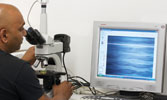
Although best practice at the production stage will prevent inner board faults from occurring, best practice at the quality control stage dictates that microsection examinations are routine. While faults are rarely found in Cirtech products, through the microscope the technician is on the lookout for no fewer than 10 different types of fault. The majority of them are related to poor drilling technique which is sometimes compounded by factors like incorrect resin curing times and poor photo-tools or photo-imaging techniques.
For single- and double-sided boards, as there are no functional internal layers, microsections are not essential and are only conducted on request. Multilayer boards are another story and microsections are carried out for every order. These microsections are carefully catalogued and archived and are kept for a minimum of two years in case any queries arise during the production or after market stages. Depending on the size of the order, at least one and possibly several sets of microsections may be taken. The frequency is determined by the square meterage being put through the plant. The microsections are harvested from each order’s overrun. For every board selected, two samples are taken from diagonally opposing corners.
In-house uses for microsections – the quest for perfection
Microsections are also used for general production line intelligence and two test boards are run through the plant each day. Samples taken from the test boards are used for quality control on the various processes in the plant. In checking electroplating quality, bonding between the laminates, hole connection, drill quality, de-smearing and connection quality from the shadow line process, Cirtech is looking for perfection rather than faults.
The information gleaned is used as a backup check on the chemical levels in the tanks. The chemistry on the production line is checked three or four times a day, depending on the square meterage throughput. The solution levels in the tanks are monitored continuously – microsections are the ultimate gauge, indicating if the plant is functioning at full efficiency.
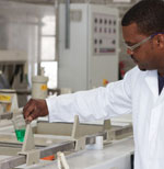
Until recently, Cirtech’s microsections were sent to a third party laboratory for scrutiny but at the end of November, the company took delivery of its own industrial microscope and now conducts inspections in-house. This speeds the process and ensures that there is no chance of miscommunication or confusion regarding samples, results and archiving.
| Tel: | +27 21 700 4900 |
| Email: | [email protected] |
| www: | www.cirtech-electronics.com |
| Articles: | More information and articles about Cirtech Electronics |


© Technews Publishing (Pty) Ltd | All Rights Reserved
 printer friendly version