


The XJTAG Development System is an established test suite with a range of software and hardware products that enable engineers to debug, test and program electronic circuits quickly and easily.
The system works with devices that conform to the IEEE 1149.1 and 1149.6 JTAG standards.
The original JTAG standard (1149.1) was conceived to allow testing of the interconnectivity of components on a printed circuit board. However, this interface is commonly used as an embedded processor debug interface and also for programming of programmable logic devices (PLDs). Advances in silicon design with increasing device densities and, in particular, the introduction of ball grid array (BGA) and chip scale packaged (CSP) devices has once again brought the use of JTAG for testing interconnectivity on printed circuit boards to the fore.
Along with this has come the need, both in development and production, for the programming of non-volatile memories (NVMs). JTAG is a serial interface which means that the ‘traditional’ method of programming NVMs using JTAG tends to be rather slow. This has led to the development of more creative programming methods. This article outlines the different programming methods available in the XJTAG Development System and shows how JTAG programming of even large NVMs can be a viable proposition in both the development and production environment.
The JTAG standard
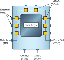
The JTAG standard requires that a JTAG cell be placed between the external pin and the internal logic of a device. The JTAG interface can then set and retrieve the values of pins without direct physical access. As well as the cells connected to the external pins, there are also control cells which select whether the pin is inputting or outputting. Often there are separate cells for input and output, so a single pin often has three JTAG cells associated with it.
The JTAG interface requires four dedicated pins on each device: one to take data onto the device (TDI), one to take data off the device (TDO), one to control what is to be done with the data (TMS) and one clock signal to synchronise the process (TCK). Data is clocked serially around the JTAG chain until a new value for each of the cells has been received, at which time it is applied to the pins. At the same time, data read from each cell is shifted out and returned to the user – see Figure 1.
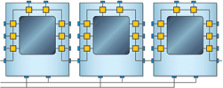
If a circuit contains more than one device that supports JTAG, they can be linked together to form a ‘JTAG chain’. In a JTAG chain, the data output from the first device becomes the data input to the second device; the control and clock signals are common to all devices in the chain. Figure 2 provides a representation of a simple JTAG chain containing three devices.
Traditional JTAG NVM programming
In the traditional method of programming NVMs, first the pins which connect to the address bus, data bus and control lines of the device to be programmed are identified and then serial data is shifted through the JTAG chain to access these pins.
As an example, when programming a Flash device which is attached to a processor, the normal address and data bus of the processor would be used. A typical processor may have more than 300 cells in its JTAG chain. A write cycle would involve one scan which sets up the address and data along with the write enable and chip select lines. The write cycle is completed by issuing a second scan which removes the write enable and chip select. Similarly, a read cycle involves a scan which sets up the address and chip select and then a second cycle which actually reads the data. A maximum TCK frequency of 10 MHz is not unusual and from this it can be seen that a single write (or read) cycle will take at least 60 μs.
Assuming a read cycle of 60 μs, it can be seen that simply reading every location in a 16-bit wide, 128 MBit Flash will take more than 8 minutes. When writing, there are usually additional sequences to be written and status flags to be polled, which means that in reality the time taken to program a Flash device using the traditional method can require much longer. Even in a development environment this can be inconvenient but in a production environment this would be unacceptable, so a different technique is required.
Processor-based programming
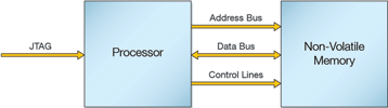
Most embedded processors have direct access to the NVMs and, as mentioned earlier, the JTAG interface is now commonly used for embedded processor debug, so this situation can be leveraged to improve NVM programming speed (see Figure 3). XJTAG supplies modules which allow access to the debug port of a processor. These modules can be used to improve NVM programming performance as well as increasing test coverage.
Most processor debug interfaces have a relatively efficient mechanism for reading and writing memory. For example, the ARM Cortex M3 processors include a memory access port which includes an auto-incrementing address register. Once the address register has been configured, reading or writing the data register results in a read or write of the memory. Once the read or write has completed, the address is automatically incremented and the next location can be read or written without having to set up the address. The JTAG chain in this case is reduced to just 35 bits long. Using the same 10 MHz TCK frequency as above, a single write cycle will take 3,5 μs. Therefore, reading the same 16-bit wide, 128 MBit Flash as above will take less than 30 seconds. Of course, if the Flash interface is 32 bits wide, this comes down to nearer 15 seconds.
Writing to the Flash is a bit more problematic since status flags have to be polled to check for write completion, which means it is not possible to use the auto-incrementing facility. This is solved by using the internal RAM of the processor to download a small program that will program the Flash from a buffer which is also held in RAM. The data to be programmed is then written, via JTAG, to the RAM buffer (using the auto-incrementing facility) and then the ARM code is called to write the buffer to Flash. The writing to Flash can usually run at the full programming speed of the Flash, so the only additional overhead is the writing of the data to the RAM buffer. This can be done 32 bits at a time and can therefore meet the same timings as for reading the Flash.
Since the processor is programming the Flash at maximum speed, the only extra delay will be the time taken to download the data, which means the extra overhead is around 15 seconds. Of course, the processor may not have sufficient RAM to buffer the entire Flash image, so there may be additional overheads involved in splitting the data into smaller buffers, but the overall gain is significant.
These improvements in programming speed are considerable and will certainly be acceptable in development and may be acceptable in production. However, not all processors can be operated in this way, so yet another alternative method may also be required.
It should be noted that in the real world, many factors conspire to mean that the programming speed does not match the theoretical maximum; one of the major factors is additional devices in the JTAG chain. According to the JTAG specifications, these other devices must implement a ‘BYPASS’ instruction which means they occupy a single bit in the JTAG chain. Unfortunately, devices in BYPASS then operate normally, which can interfere with the programming process (since they might be accessing the address and data bus).
Some devices might implement a ‘CLAMP’ instruction which holds all the pins in a given state whilst only occupying a single bit in the JTAG chain. Unfortunately, some devices have to be held in EXTEST which means all of their JTAG cells are in the chain and have to be maintained in a state which stops them interfering with the programming. This can significantly increase the programming time.
PLD-based programming
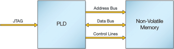
Many modern electronic designs include PLDs. If a PLD has full access to the NVM and can also be programmed to take control of the JTAG chain, the PLD can be used to program the NVM (see Figure 4). XJTAG provides the ‘XJFlash’ module which uses the onboard PLD to take control of the JTAG chain and program an attached NVM.
The technique used is similar to the technique used to program the PLD itself. The PLD is programmed to take control of the JTAG chain. A simple protocol is then operated over the JTAG chain which means the programming data can be transferred with virtually no overhead at all. The programming data for the 128 MBit example above can be transferred in less than 14 seconds, which can occur in parallel to the actual programming of the Flash device. Of course, this data rate is usually too fast for the Flash programming speed and PLDs rarely have enough memory space to buffer an entire Flash image. As a result, the image is usually split into blocks and the protocol includes a mechanism to allow the system to wait for more buffer space to become available in the PLD before sending the next block.
As mentioned in the processor based example, additional devices in the chain can affect the programming speed. However, since the PLD-based programming method makes much more efficient use of the JTAG chain data, the effect is greatly reduced.
Practical example
This example uses the Orion Demo Platform as supplied by Micron. The board has two JTAG chains: one has an Intel/Marvell PXA270 processor and the other has a Xilinx Spartan 3 FPGA and a Xilinx XCF08P PROM. The board also has a PISMO 2 connector which is accessible from the Spartan 3. For the purposes of this example, a Micron Omneo phase change memory (PCM) module was plugged into the PISMO 2 port (see Figure 5).
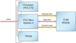
Although it would be possible to just use the single JTAG chain which includes the Spartan 3, the PXA270 can be put into CLAMP mode which only adds one bit to the chain. The PXA270 is also used for connection integrity checking so it was left in the chain. The PROM can also be put into CLAMP mode, so again only contributes a single bit to the chain.
The Spartan 3 was programmed with XJFlash and a 128 MBit file was generated and filled with pseudo random data. This file was then used to program the PCM module using XJRunner to control access to the XJFlash high-speed programming system.
The PCM module has various modes of operation. Since PCM devices are bit-alterable, there is no need for an erase operation before programming. However, there is a slight speed advantage if the device is known to be all 1s when programming.
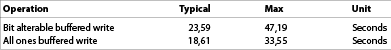
Using a TCK frequency of 20 MHz, the time taken to program the device is as shown in Table 1. The theoretical programming times for the device are shown in Table 2. As can be seen from these tables, the actual programming figure is faster than the theoretical ‘typical’ figure. By observing the state of the programming buffers, it was possible to confirm that the buffers, once filled, were not seen empty again until programming had completed. This shows that the limitation was the PCM device programming speed and not the JTAG interface.
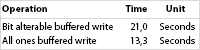
The time taken to verify the programming for the above device was 9 seconds which again is close to the theoretical minimum time given the TCK frequency.
Conclusion
Whilst programming of NVMs using the traditional method of JTAG programming is certainly possible, the slow speed makes it only really viable for small images. NVMs are usually directly attached to a processor which means that, with the help of the processors debug port, it is possible to greatly speed up the programming of NVMs.
If the NVM’s address bus, data bus and control lines are attached to a suitable PLD, the PLD can be programmed to program JTAG data straight into the NVM. This technique allows many NVMs to be programmed in the shortest time possible. If NVM programming speed over JTAG is an issue, there are alternatives that can greatly improve programming speed but they are dependent on the specific application.
| Tel: | +27 11 315 8316 |
| Email: | [email protected] |
| www: | www.asic.co.za |
| Articles: | More information and articles about ASIC Design Services |


© Technews Publishing (Pty) Ltd | All Rights Reserved
 printer friendly version