


Ever since the first watermills and windmills were used to generate electricity, energy harvesting has been an attractive source of energy with great potential.
In recent years, energy harvesting technology has become more sophisticated and efficient, and energy storage technologies, such as supercapacitors and thin-film batteries (TFBs), have become more cost-effective.
Among the final pieces in the energy harvesting solution jigsaw puzzle are integrated circuits that can perform useful functions such as algorithmic control and wireless communications using tiny amounts of energy. We have now reached a technological tipping point that will result in the evolution of energy harvesting-based systems from today’s niche products, such as calculators and wrist watches, to their widespread use in building automation, security systems, embedded controls, agriculture, infrastructure monitoring, asset management and medical monitoring systems.
The wireless sensor node is one of the most important product types being forecast for growth as an energy harvesting solution. Wireless sensors are ubiquitous and very attractive products to implement using harvested energy. Running mains power to wireless sensors is often neither possible nor convenient, and, since wireless sensor nodes are commonly placed in hard-to-reach locations, changing batteries regularly can be costly and inconvenient.
It is now possible to implement wireless sensors using harvested energy because of the off-the-shelf availability of ultra-low-power, single-chip wireless microcontrollers (MCUs) capable of running control algorithms and transmitting data using sophisticated power management techniques.
Low-power optimisation
Low-power modes on MCUs and wireless transceivers have been optimised in recent years to enable effective power manage-ment in wireless sensor applications. Figure 1 illustrates a typical wireless sensor node power cycle.
The designer’s objective is to minimise the area under the curve in Figure 1, which corresponds to power consumption. Power consumption can be minimised by optimising the relative amount of time spent in low-power sleep mode and reducing the active mode time. A fast processing core enables the MCU to execute the control algorithm very quickly, enabling a rapid return to low-power sleep mode and thereby minimising the power-hungry area under the curve.
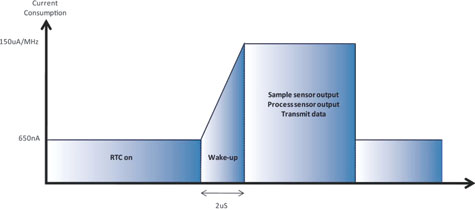
Wireless sensor nodes spend most of their time in sleep mode. The only subsystem that stays awake is the real-time clock (RTC). The RTC keeps time and wakes up the wireless sensor node to measure a sensor input. Low-power RTCs typically integrated onto microcontrollers consume only a few hundred nanoamperes. It is important to minimise the system’s wake-up time because power is consumed during this time.
An RTC uses a free-running counter in the MCU timer subsystem. When the free-running counter rolls over, it generates an interrupt that wakes up the MCU often. If a 32,768 kHz crystal is used, a 16-bit free-running counter rolls over every two seconds and wakes up the MCU. If a wider free-running counter, such as a 32-bit counter, is used, the periodic interrupt occurs less often and additional power may be conserved.
When a wireless sensor node wakes up, it is usually intended to measure a sensor signal using the analog-to-digital converter (ADC). It is important to note the wake-up time of the ADC as well as the digital wake-up time since there is little point in waking up the CPU very quickly if the ADC takes an order of magnitude longer to wake up. A low-power MCU should wake up both the CPU and the ADC in a couple of microseconds.
When the sensor node is awake, the MCU current is typically approximately 160 μA/MHz. When the sensor data has been measured, the algorithm running in the MCU decides whether the data should be transmitted by the radio. To send the data, a low-power ISM band radio consumes somewhat less than 30 mA for only a millisecond or so. When this peak current is averaged out, the overall average current consumption of the wireless sensor node is in the low microampere range.
The radio transmission consumes most of the current in the system. Minimising the amount of time the radio is on is essential to conserving energy. One way to achieve this is to avoid complicated communications protocols that require the transmission of many bits of data. Steering clear of standards with large protocol overhead is desirable when power is at a premium. It is also important to consider the desired range. Wireless range can be traded for power consumption.
An interesting approach to balancing this trade-off is to use dynamic ranging, which allows full-power transmissions when maximum energy is available but reduces the output power level when harvested energy is limited. Another way to reduce the wireless sensor node’s power consumption is to minimise the number of chips used in the system. Fewer chips on the printed circuit board (PCB) result in lower leakage current losses.
Using an MCU that integrates as many functions as possible ultimately helps reduce overall current consumption. If a DC-DC converter is integrated onto the MCU, it can be switched off when the MCU is sleeping. Silicon Labs’ Si10xx wireless MCU, for example, contains an integrated DC-DC converter that allows the system to be powered by a single AAA alkaline battery and still achieve 13 dB output power at the antenna. Because of their high level of integration and low power consumption, the Si10xx wireless MCUs have been used successfully in energy harvesting wireless sensor nodes.
Managing harvested energy
An important consideration in the development of an energy harvesting sensor node is to ensure that there is always enough energy available to power the system, as shown in Figure 2.
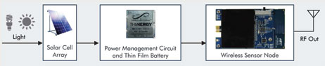
This energy harvesting system uses a solar cell array to harvest energy. A solar cell unit, such as a Sanyo AM-1815, delivers approximately 40 μA when a 200 Lx light level is available. It is reasonable to expect this level of light in an office with a window but no direct sunlight on the cell. The 40 μA of current that the array generates is fed into a power management circuit and trickle-charged into a thin-film battery (TFB).
When selecting power management chips, it is necessary to pay attention to the leakage current characteristics, which are normally only a few microamperes. However, with only 40 μA coming into the TFB, this tiny amount of leakage must be understood and accounted for. A thin-film battery, such as the Infinite Power Solutions MEC101-7SES, provides a 0,7 mAh capacity, which is a reasonable amount of energy for a wireless sensor node system. At a 200 Lx level of light, this TFB charges up fully in around 17,5 hours.
This combination of solar cell, power management and storage technologies provides an adequate level of energy for a wireless sensor node. The next important decision in the design process is the selection of a low-power MCU and wireless transceiver combination that can operate effectively from a limited energy source. A Silicon Labs Si1012 wireless MCU is a suitable choice because of its low power consumption and high-performance radio characteristics. This wireless MCU uses a programmable sub-GHz ISM radio in a single-chip configuration with an ultra-low-power MCU; the highly-integrated device, which also includes an on-chip temperature sensor, is essentially a wireless sensor node on a chip.
With the hardware configured as shown in Figure 2, the control problem to be considered is how to operate the wireless sensor node at a duty ratio that does not deplete the TFB capacity that is itself being trickle-charged by the solar cell. Using the low-power design techniques discussed earlier, it is possible to reduce the average current of the wireless sensor node to around 51 μA (including power management leakage) while transmitting sensor data every second for three minutes. That is low enough to allow the system to operate and stay fully charged in minimal lighting conditions.
If the light input is reduced to 0 Lx, the wireless sensor node continues to operate and transmit for 64 hours before the TFB capacity is exhausted (assuming the three-minute transmit period is repeated every 20 minutes). A simple spreadsheet detailing expected input energy (ie, how much light is available) versus output energy (how often the node is required to transmit) is the only tool that a designer needs to optimise the system. If more than adequate light is expected, this energy can be used to increase the range of the transmitter. This type of system allows a range up to 100 metres, depending on the exact conditions.
Many different types of energy harvesting sources can be used to power a wireless sensor node instead of using a solar cell (or even in combination with solar energy). If a wireless sensor node is placed in a location without ready access to a light source, the node can be powered by thermal, vibration (piezoelectric) or radio wave energy harvesting sources. The power management, storage and wireless sensor node circuits are essentially the same as those used in the solar cell example.
Regardless of the harvested energy source, the system design principles are the same: a limited source of energy is captured and stored in a TFB and then used to power an ultra-low-power wireless sensor node.
Summary
The ability to power wireless sensor nodes from harvested energy sources allows embedded designers to offer systems with significantly reduced cost of ownership for the end-user as well as benefits to the environment. The cost of replacing batteries housed in out-of-the-way sensor node locations can be quite significant. These wireless sensor nodes, for example, can be embedded in structures such as buildings or bridges, or even buried underground.
The three key enabling technologies needed to create self-sustaining wireless sensor nodes are readily available today: cost-effective energy harvester devices, small and efficient energy storage devices and single-chip, ultra-low-power wireless MCUs. Wireless sensor nodes powered by harvested energy sources will soon become commercially viable and commonplace technologies used in our homes, offices, factories and infrastructure.
For more information contact Gary de Klerk, NuVision Electronics, +27 (0)11 894 8214, [email protected], www.nuvisionelec.co.za
| Tel: | +27 11 608 0144 |
| Email: | [email protected] |
| www: | www.nuvisionelec.com |
| Articles: | More information and articles about NuVision Electronics |


© Technews Publishing (Pty) Ltd | All Rights Reserved
 printer friendly version