


Hostile environments found in automotive, military and avionic applications push integrated circuits to their technological limits, requiring them to withstand high voltage and current, extreme temperature and humidity, vibration, radiation and a variety of other stresses.
Systems engineers are rapidly adopting high-performance electronics to provide features and functions in application areas such as safety, entertainment, telematics, control and human-machine interfaces.
The increased use of precision electronics comes at the price of higher system complexity and greater vulnerability to electrical disturbances including over-voltages, latch-up conditions and electrostatic discharge (ESD) events.
Because electronic circuits used in these applications require high reliability and high tolerance to system faults, designers must consider both the environment and the limitations of the components that they choose.
In addition, manufacturers specify absolute maximum ratings for every integrated circuit; these ratings must be observed in order to maintain reliable operation and meet published specifications.
When absolute maximum ratings are exceeded, operational parameters cannot be guaranteed; and even internal protections against ESD, over-voltage or latch-up can fail, resulting in device (and potentially further) damage or failure.
This article describes challenges engineers face when designing analog switches and multiplexers into modules used in hostile environments, and provides suggestions for general solutions that circuit designers can use to protect vulnerable parts.
It also introduces some new integrated switches and multiplexers that provide increased over-voltage protection, latch-up immunity and fault protection to deal with common stress conditions.
Standard analog switch architecture
To fully understand the effects of fault conditions on an analog switch, we must first look at its internal structure and operational limits.
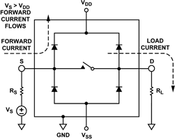
A standard CMOS switch (Figure 1) uses both N- and P-channel MOSFETs for the switch element, digital control logic and driver circuitry. Connecting N- and P-channel MOSFETs in parallel permits bidirectional operation, allowing the analog input voltage to extend to the supply rails, while maintaining fairly constant on-resistance over the signal range.
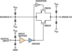
The source, drain and logic terminals include clamping diodes to the supplies to provide ESD protection, as illustrated in Figure 1. Reverse-biased in normal operation, the diodes do not pass current unless the signal exceeds the supply voltage. The diodes vary in size, depending on the process, but they are generally kept small to minimise leakage current in normal operation.
The analog switch is controlled as follows: the N-channel device is on for positive gate-to-source voltages and off for negative gate-to-source voltages; the P-channel device is switched by the complementary signal, so it is on at the same time as the N-channel device. The switch is turned on and off by driving the gates to opposite supply rails.
With a fixed voltage on the gate, the effective drive voltage for either transistor varies in proportion to the polarity and magnitude of the analog signal passing through the switch.
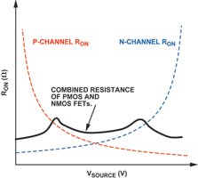
The dashed lines in Figure 2 show that when the input signal approaches the supplies, the channel of one device or the other will begin to saturate, causing the on-resistance of that device to increase sharply. The parallel devices compensate for one another in the vicinity of the rail voltages, however, so the result is a fully rail-to-rail switch, with relatively constant on-resistance over the signal range.
Absolute maximum ratings
Switch power requirements, specified in the device data sheet, should be followed in order to guarantee optimal performance, operation and lifetime. Unfortunately, power supply failures, voltage transients in harsh environments, and system or user faults that occur in the course of real-world operation may make it impossible to meet data sheet recommendations consistently.
Whenever an analog switch input voltage exceeds the supplies, the internal ESD protection diodes become forward-biased, allowing large currents to flow, even if the supplies are turned off, causing ratings to be exceeded.
When forward-biased, the diodes are not rated to pass currents greater than a few tens of milliamperes; they can be damaged if this current is not limited. Furthermore, the damage caused by a fault is not limited to the switch but can also affect downstream circuitry.
The Absolute Maximum Ratings section of a data sheet (Figure 3) describes the maximum stress conditions a device can tolerate; it is important to note that these are stress ratings only.
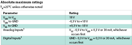
Exposure to absolute maximum ratings conditions for extended periods may affect device reliability. The designer should always follow good engineering practice by building margin into the design. The example here is from a standard switch/multiplexer data sheet.
In this example, the VDD to VSS parameter is rated at 18 V. The rating is determined by the switch’s manufacturing process and design architecture. Any voltage higher than 18 V must be completely isolated from the switch, or the intrinsic breakdown voltages of elements associated with the process will be exceeded, which may damage the device and lead to unreliable operation.
Voltage limitations that apply to the analog switch inputs – with and without power supplies – are often due to the ESD protection circuitry, which may fail as a result of fault conditions.
Analog and digital input voltage specifications are limited to 0,3 V beyond VDD and VSS, while digital input voltages are limited to 0,3 V beyond VDD and ground. When the analog inputs exceed the supplies, the internal ESD protection diodes become forward-biased and begin to conduct.
As stated in the Absolute Maximum Ratings section, over-voltages at IN, S or D are clamped by internal diodes. While currents exceeding 30 mA can be passed through the internal diodes without any obvious effects, device reliability and lifetime may be reduced, and the effects of electromigration, the gradual displacement of metal atoms in a conductor, may be seen over time.
As heavy current flows through a metal path, the moving electrons interact with metal ions in the conductor, forcing atoms to move with the flow of electrons. Over time this can lead to open or short circuits.
When designing a switch into a system, it is important to consider potential faults that may occur in the system due to component failure, user error or environmental effects. The next section will discuss how fault conditions that exceed the absolute maximum ratings of a standard analog switch can damage the switch or cause it to malfunction.
Common fault conditions, system stresses and protection methods
Fault conditions can occur for many different reasons; some of the most common system stresses and their real-world sources are shown in Table 1.
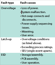
Some stress may not be preventable. Regardless of the source of the stress, the more important issue is how to deal with its effects. The questions and answers below cover these fault conditions: over-voltages, latch-up and ESD events – and some common methods of protection.
Over-voltage
What is an over-voltage condition?
Over-voltage conditions occur when analog or digital input conditions exceed the absolute maximum ratings. The following three examples highlight some common issues designers need to consider when using analog switches.
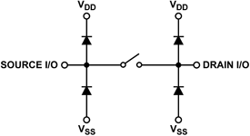
Loss of power with signals present on analog inputs (Figure 5).
In some applications, the power supply to a module is lost, while input signals from remote locations may still be present. When power is lost, the power supply rails may go to ground, or one or more may float. If the supplies go to ground, the input signals can forward-bias the internal diode, and current from the switch input will flow to ground, damaging the diode if the current is not limited.
If loss of power causes the supplies to float, the input signals can power the part through the internal diodes. As a result, the switch – and possibly any other components running from its VDD supply – may be powered up.
Over-voltage conditions on analog inputs
When analog signals exceed the power supplies (VDD and VSS), the supplies can be pulled to within a diode drop of the fault signal. Internal diodes become forward-biased and currents flow from the input signal to the supplies. The over-voltage signal can also pass through the switch and damage parts downstream. The explanation for this can be seen by considering the P-channel FET (Figure 6).
A P-channel FET requires a negative gate-to-source voltage to turn it on. With the switch gate equal to VDD, the gate-to-source voltage is positive, so the switch is off. In an unpowered circuit, with the switch gate at 0 V or where the input signal exceeds VDD, the signal will pass through the switch, as there is now a negative gate-to-source voltage.
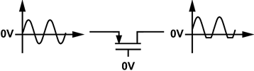
Bipolar signals applied to a switch powered from a single supply
This situation is similar to the previously described over-voltage condition. The fault occurs when the input signal goes below ground, causing the diode from the analog input to ground to forward-bias and current to flow.
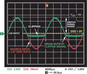
When an AC signal, biased at 0 V d.c., is applied to the switch input, the parasitic diodes can be forward-biased for some portion of the negative half-cycle of the input waveform. This happens if the input sine wave goes below approximately –0,6 V, turning the diode on and clipping the input signal, as shown in Figure 7.
This article will be continued in the next edition of Dataweek. The next part concludes the topic of over-voltage and delves into latch-up and ESD.
| Tel: | +27 11 923 9600 |
| Email: | [email protected] |
| www: | www.altronarrow.com |
| Articles: | More information and articles about Altron Arrow |


© Technews Publishing (Pty) Ltd | All Rights Reserved
 printer friendly version