


Mark Jackson, of magnetics vendor Pulse, looks at the basics of surface-mount chip inductors and highlights some design considerations.
Surface-mount chip inductor types
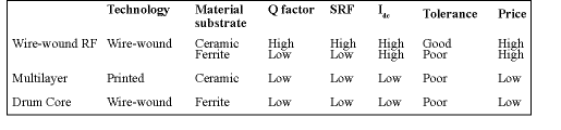
There are basically three varieties of chip inductor in common use: wire-wound RF, multilayer and drum-core. The primary differences between these competing types are the core material used to enhance the inductance of the coil, and the construction method. In the wire-wound RF and drum-core types, the wire is wound around a ceramic or ferrite bobbin whereas in the multilayer device the coil is formed by interconnecting layers of conductive material printed on a ceramic substrate.
Table 1 compares the performance merits of surface-mount chip inductor types. Although wire-wound RF types are more expensive, price is not the only consideration - RF engineers must also consider the needs of the application in terms of Q factor, Idc (maximum current carrying capacity), Rdc (resistance at DC), tolerance and SRF (self resonant or series resonant frequency). As the table shows, all of these parameters favour the ceramic core wire-wound.
Inductor basics
Chip inductors are formed by winding a wire around a ceramic or ferrite core to increase the magnetic flux linkage between the turns of the coil. The majority of high frequency inductors used above 50 MHz are formed on a ceramic bobbin or substrate. Nonmagnetic cores such as these exhibit the opposite effect to a magnetic core in that they reduce rather than increase the inductance of the coil. Ceramic cores are mainly used to reduce the RF core losses as the high frequency currents mainly flow near the surface of the conductor. The resistance that a conductor offers to the high frequency alternating current is much greater than the resistance of the same conductor to direct current (DC) and is known as the 'skin effect'. The skin effect is a characteristic of conductors that carry alternating current but is much more pronounced in coils than in straight conductors.
The skin effect causes the current in the conductor to be much denser near the surface of the conductor than at its centre. Consequently, as the instantaneous value of the alternating current changes, the inductance of a conductor in its interior is much greater than the instantaneous inductance near its surface. The result is that more current flows near the surface or 'skin' of the conductor than at its centre. Since the reactance of the coil increases proportionally to the increasing frequency, the skin effect also increases as the frequency is increased. A high skin effect degrades the 'Q' of the inductor as frequency increases (See later - 'Q factor/SRF').
Another source of loss is the dielectric material used to form the body of the inductor. There is no perfect insulator and so dielectric losses cannot be avoided at very high frequencies. Dielectric losses, like skin effect, also tend to increase the effective resistance of a coil at high frequencies. Inductors are probably the component most susceptible to changing performance over frequency and Figure 1 illustrates what a real-world inductor looks like at RF frequencies and shows the resultant equivalent circuit.
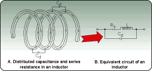
Figure 1A shows how capacitive coupling (Cd) can occur between two wires when in close proximity to one another and only separated by a dielectric. The resistance (Rs) represents the wire resistance that exists in a wire. Figure 1B shows a representation of the lumped resistive, capacitive and inductive component elements of an inductor.
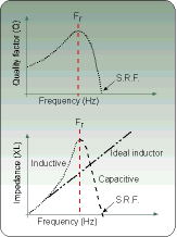
The effect of Cd can have a dramatic effect upon the impedance of the inductor as illustrated in Figure 2, because 'fringe' effects become dominant at high frequencies. At low frequencies the inductor's reactance parallels that of an ideal inductor. With increasing frequency the reactance of the inductor departs from the ideal curve and increases at a much faster rate until it reaches a peak value at the inductor's parallel resonant frequency (Fr). Above Fr the inductor's reactance begins to decrease with increasing frequency and thus the inductor begins to look like a capacitor. The series resistance (Rs) of the coil prevents the impedance of the inductor from reaching infinity at resonance (Fr). Another effect of Rs is to broaden the resonant peak of the impedance curve at Fr.
Comparisons made between inductors at near to Fr will produce an inaccurate representation of the inductor's performance. This can lead to problems in the end application since the performance of one inductor to another may vary quite markedly since the performance of the inductor is dominated by the parasitic content (distributed capacitance Cd) of the inductor.
Q factor/SRF
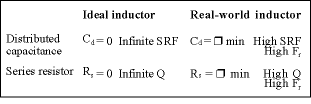
The ratio of an inductor's reactance (XL) to its series resistance (Rs) is often used as a measure of the quality factor of the inductor. The larger the ratio the better the inductor. The quality factor is often referred to as the 'Q' of the inductor. If the inductor were constructed from a perfect conductor (zero loss), its Q would be infinite. Of course this is impossible and so the Q of an inductor always has some finite value.
The Q factor, Fr and SRF of an inductor are directly linked to one another since if the test frequency is near Fr or SRF, the inductor results may be misleading by very wide margins since the result is dominated by distributed capacitance reactance. To overcome this, the test frequency of the inductor is normally located at a point on the inductor's curve where the reactance of the inductor approaches that of an ideal inductor. At this point on the curve the component to component variations are kept to a minimum since the parasitic contribution (Cd) is also at a minimum. To guard against this problem RF engineers should select an inductor with the highest test frequency possible to guarantee the quality of the inductor.
At low frequencies the Q of an inductor is very good because the only resistance in the winding is the DC resistance of the wire which is very small (Figure 2). As mentioned earlier, as the frequency increases, the skin effect increases to degrade the Q of the inductor. At low frequencies the Q increases directly inline with the reactance (XL) since the skin effect has not become noticeable. The Q continues to rise but as the frequency approaches Fr the skin effect starts to become dominant, reducing the rate of increase. At Fr the series resistance and reactance are increasing at the same rate. Above Fr the distributed capacitance Cd and skin effect of the winding combine together to decrease the Q of the inductor to zero at SRF.
Understanding inductor curves
RF design engineers require inductors to meet the following requirements:
* Low cost.
* Compatibility with the competition:
-- Q, SRF and usable frequency range => competition.
* Small component-to-component variation.
* Performance approaches that of an ideal inductor:
-- High Q (low series resistance).
-- High SRF (low distributed capacitance).
Determining the inductor equivalent circuit
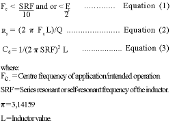
To determine the inductor equivalent circuit an RF engineer must deduce the value of Rs and Cd from the curves supplied by the inductor manufacturer. To do this the following equations can be used. Of course the values deduced only apply at one specific frequency. Also the frequency at which the inductor is used within the application must be an order of magnitude (divided by 10) below the SRF and preferably not nearer than 0,5 Fr.
Conclusion
As a major vendor of chip inductors to the telecoms and networking industry, Pulse has seen a recent dramatic increase in shipments of ceramic wire-wound chip inductors. Why should this be?
* Whilst there is no perfect component, they provide the closest match to an ideal inductor. Although the performance of multilayer chip inductors has improved, it is unlikely to reach that of a ceramic wire-wound product.
* The price differential between multilayer and ceramic wire-wound chip inductors has reduced due to improvements in manufacturing and Pulse's ability to leverage its strength as the industry leader for magnetic-based products.
* RF engineers need also to consider the needs of the application in terms of Q factor, Idc (maximum current carrying capacity), Rdc (resistance at DC), tolerance and SRF (series resonant frequency) and not on price alone.
* With the ongoing digital revolution, system demands for improved linearity necessitate the requirement for components with reduced parasitic content.
Chip inductor information can be obtained from the Pulse website on www.pulseeng.com/scripts/finder/rfind/mcis.cfm
For further information contact Memec SA, (021) 674 4103.


© Technews Publishing (Pty) Ltd | All Rights Reserved
 printer friendly version