


When one thinks about applications for modern power MOSFETs using trench technology, running them in linear mode may not be top of the priority list. Yet there are multiple uses for trench power MOSFETs in linear mode. In fact, even turning the power MOSFET on and off in switching applications is a form of linear operation.
Also, these components can be run in linear mode to protect the device against voltage surges. This article will illustrate the factors that need to be considered for linear operation and show how trench power MOSFETs are suited to it.
Modern trench power MOSFETs are mainly used in switching applications such as DC-DC converters and motor control using pulse width modulation (PWM). In other words, the power MOSFET is alternately switched on completely, then switched off completely.
To maximise efficiency and minimise losses when the components are switching, the technology needs to be optimised to cope with static and dynamic power dissipation. This is why development of new technologies focuses on parameters like on-resistance (RDS(on)), gate charge (QG) and capacities (Ciss, Coss, Crss).
Safe operating area
But how can modern trench power MOSFETs be used in linear mode? What we mean by linear in this context is a mode of operation in which the power MOSFETs are neither completely switched on nor completely switched off. Small changes to the gate-source voltage (VGS) can have a significant effect on the drain current (ID) and higher drain-to-source voltages (VDS) might coincide with large drain currents.
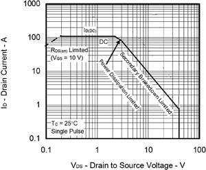
Many power MOSFET datasheets show diagrams indicating the safe operating area (SOA) and these are very helpful when deciding whether or not linear mode is feasible. Figure 1 shows an example of the maximum drain voltage (ID) in relation to the drain source voltage (VDS), when the power MOSFET is run in linear mode (in this case, DC).
Trench power MOSFETs can operate below the SOA curve with no constraints, as long as the curve’s limiting factors have been correctly indicated in the datasheet as relates to the following points:
1. On-resistance limit (RDS(on) limit): the maximum current for the relevant VDS is limited by the component’s RDS(on), so its intrinsic properties will stop it from exceeding this limit.
2. Package limit (ID(DC)): the maximum current is limited by package constraints.
3. Power dissipation limit: the power MOSFET’s maximum channel temperature (usually 175°C) must not be exceeded. As the power dissipation causes an increase in the channel temperature, it should be kept in check to ensure that the temperature does not rise above this level.
4. Hotspot, also known as the Spirito limit (secondary breakdown limit): tiny flaws, like non-homogeneities in the chip’s cell structure or small solder cavities, can cause an uneven distribution of the current over the chip. As a result, some of the chip’s cells may carry more current and become hotter than the surrounding cells. This thermal instability can lead to the temperature of the affected cells increasing to well above the maximum permitted channel temperature level, which in turn will destroy the component. This is known as the Spirito effect[1] and can occur in larger ID/VDS combinations. It is vital to take this into account when putting together the SOA. The Spirito effect can occur at levels above the line, but no hotspots will occur below it, avoiding thermal instability and the destruction of the component.
5. Breakdown voltage: this is the component’s specified breakdown voltage.
There are additional parameters that have a major influence on the SOA curve, including the time that the component is operating in linear mode and the surrounding temperature (TA).
The left side of Figure 2 shows the whole SOA diagram of the NP109N04PUJ trench power MOSFET at room temperature and for various linear mode timescales. It is clear from the diagram that the SOA increases for short periods, allowing for higher ID-VDS combinations. As a result, the package can tolerate short pulses of higher currents, and short pulses shift the power dissipation and Spirito limits to higher levels.
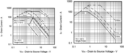
Conversely, the SOA becomes smaller at higher surrounding temperatures because the maximum power dissipation level decreases as the temperature increases. This effect is shown in Figure 2 (right) for a surrounding temperature (TA) of 125°C. The maximum power dissipation limit shifts the curves down to lower levels.
Linear mode applications
Time and surrounding temperatures are decisive factors for operation in linear mode, and the following examples include a variety of timescales and temperatures:
1. Switching application, linear mode in the μs range.
2. Active clamp, linear mode in the ms range.
3. Linear regulator, DC operation.
1. Switching application
Switching is by far the most common application for trench power MOSFETs, which are used in DC-DC converters as well as in PWMs for motor controllers. Strictly speaking, the power MOSFET is running in linear mode when it is being switched on as well as off. The switching times vary from a few hundred nanoseconds up to the millisecond range or even longer.
The left diagram in Figure 3 shows a typical switch-on procedure with a PWM at 20 kHz, often used for the control of brushless DC (BLDC) motors. Within about 1 μs, ID increases to the maximum level of 70 A, while VDS decreases to the on-state value VDS=RDS(on)*ID = 120 mV.
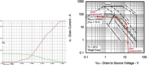
The right-hand diagram in Figure 3 shows that the current-voltage characteristic of this switching operation has been added to the room-temperature SOA of the NP109N04PUJ. Here it can be clearly seen that the data values are located above the DC curve but still well within the SOA for short periods. As a result, this type of switching operation is feasible with no constraints.
2. Active clamp operation
During the switching of inductive loads, high-voltage peaks occur during the power MOSFET’s switch-off process because the inductance is trying to maintain the flow of current.
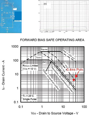
The active clamp operation is used to stop the power MOSFET from avalanching (Figure 4). This involves using a Zener diode and a conventional diode between the drain and gate connectors, where the Zener voltage is lower than the power MOSFET’s breakdown voltage.
If there is a voltage peak at the drain, the Zener diode will maintain the Zener voltage and the gate potential will be increased, putting the power MOSFET into linear mode. In this way, the inductive energy can be dissipated safely.
In this example, the drain current (ID) of 5 A is switched off. The Zener diode limits the drain voltage to about 30 V and the power MOSFET goes into linear mode (VGS ~4 V). The duration of this linear operation is about 0,4 ms and the current-voltage characteristic is still below the 1 ms curve.
3. Linear voltage regulator
Along with DC-DC converters – which are increasingly being used as voltage converters due to their high efficiency levels – linear voltage regulators are also being used in automotive applications. Here, the power MOSFET is used to transform the input voltage to a lower output voltage. By varying the gate voltage, the voltage drop VDS can be regulated, putting the power MOSFET into DC linear mode.
With a surrounding temperature of 125°C, the linear regulator changes the input voltage of 6,5 V to 1,2 V, providing output voltage of 5 A.
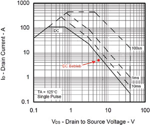
Accordingly, the drain-to-source voltage VDS is 5,3 V. Figure 5 shows the SOA diagram at 125°C, demonstrating that the NP109N04PUJ can be used as a linear regulator with no constraints because the current/voltage levels are all below the 125°C DC curve.
Conclusion
There is nothing to stop designers using trench power MOSFETs in applications with linear operation; they are also suitable for DC applications. To decide whether or not a component can be used in a specific use case, the SOA diagrams provided in the power MOSFET’s datasheet should indicate all limiting factors and the Spirito effect, in particular, must be taken into account.
Reference
[1] Breglio G.; Frisina, F.; Magri, A.; Spirito, P.: 'Electro-Thermal Instability in Low-Voltage power MOS: Experimental Characterisation', 1999 IEEE ISPSD 1999, p. 233-236.
For more information contact Marinus Rudman, Hi-Q Electronics, +27 (0)21 595 1307, [email protected], www.hi-q.co.za
| Tel: | +27 21 595 1307 |
| Email: | [email protected] |
| www: | www.hi-q.co.za |
| Articles: | More information and articles about Hi-Q Electronics |


© Technews Publishing (Pty) Ltd | All Rights Reserved
 printer friendly version