


Large stacks of series-connected battery cells are increasingly used to power electric vehicles or store energy in wind and solar power systems.
It is not uncommon to have 100 cells connected in series in an electric vehicle, and even more in energy storage units for alternative energy systems.
Typically, the stack is treated by the charge-discharge system as a single battery: cells are charged and discharged as a series stack and the state of charge (SOC) of each cell depends on its ability to store and maintain charge. Treating the cell stack as a single battery composed of capacity-matched cells can work well in the short term, but becomes increasingly inefficient in the long run.
When a battery stack is first constructed, the capacities of its component cells can be well matched, but over time, individual cells lose capacity at different rates due to temperature variations and other factors. In a straightforward stack charge-discharge implementation, the cell with the least capacity – the weakest cell – effectively limits the run time of the stack. When the stack is charged, the weakest cell reaches its full charge voltage before stronger cells, so stronger cells are not charged to capacity. Likewise, when the stack is discharged, the weakest cell reaches its cutoff voltage sooner, limiting run time.
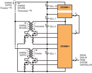
The capacity of the stack and its run time can be improved by balancing the state of charge between cells within the stack. Figure 1 shows a simplified schematic of a 12-cell balancer using two LTC3300-1 cell balancing controllers.
Using the LTC3300-1 to improve battery stack run times and lifetimes
The LTC3300-1 is a fault-protected controller IC for transformer-based bidirectional active balancing of multicell battery stacks. Active bidirectional balancing can transfer charge from the stack to low SOC cells, or transfer charge from high SOC cells to the stack. In this way, the overall capacity of the stack is improved.
A single LTC3300-1 can balance up to six series connected cells with a common mode voltage range of up to 36 V. Multiple LTC3300-1 devices can be connected in series, allowing balancing of long strings of series connected cells. A unique level shifting SPI-compatible serial interface allows multiple LTC3300-1 devices to be connected in series without optocouplers or isolators.
As the stack is charged, weaker cells operate in discharge mode and stronger cells operate in the charge mode until all cells reach their full SOC. Likewise, during discharge, weaker cells are operated in charge mode while stronger cells are operated in discharge mode until all cells reach their cutoff voltage. This extends the run time of the stack, which reduces the number of charge/discharge cycles and thus extends the life of the batteries within the stack.
With the LTC3300-1, all individual cell balancers can operate simultaneously in any combination of discharge or charge modes, even when multiple LTC3300-1 devices are used. For instance, for a stack of 12 cells, with two LTC3300-1 devices connected in series, charge can be transferred from cell 12 to cell 1 in a single time step by discharging cell 12 and charging cell 1.
When compared to other methods of transferring charge between cells, this single time step method is the fastest and most efficient. A single time step can include multiple balancers in discharge or charge modes, resulting in optimum balance time.
The LTC3300-1 includes fault protection, including read-back capability, cyclic redundancy check (CRC) communication error detection, maximum on-time volt-second clamps and cell or transformer secondary over-voltage shutdown.
How to apply the LTC3300-1
The cell balancer incorporates a boundary mode synchronous flyback transformer power stage that is controlled by the LTC3300-1. There are six sets of control signals within the LTC3300-1 that control the gates of the primary side and secondary side NMOS switches, and current sense inputs for each pair of NMOS switches.
The naming convention used for the LTC3300-1 is that the transformer primary is connected across the battery cell and the secondary of the transformer is across the ground reference of the IC to a point six or more cells up the stack. The primary side gate signals are referenced to the next lower cell while the secondary side gates are referenced to the ground reference of the IC, the V- exposed pad.
During discharge mode (Figure 2) the primary side NMOS is turned on first and remains on until the current signal ramps up to 50 mV or the primary max on-time setting is reached. The flux built up in the primary side of the flyback transformer is then transferred to the secondary. The secondary gate signal turns on the secondary side NMOS, and it remains on until the secondary current sense signal ramps down to 0 mV or the secondary side max on-time is reached.
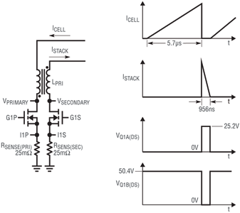
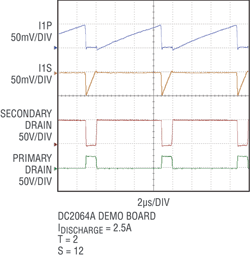
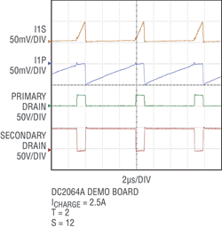
The cycle repeats until the LTC3300-1 is given a command to stop the discharge mode or encounters a fault such as a watchdog timer time-out, a cell under-voltage (2,0 V), a cell over-voltage (5,0 V) or a transformer secondary over-voltage caused by a lost connection. During charge mode (Figure 3) the secondary is turned on first and remains on until the secondary current signal ramps up to 50 mV or the secondary max on-time setting is reached.
The flux built up in the secondary side of the flyback transformer is then transferred to the primary. The primary gate signal turns on the primary side NMOS and it remains on until the current sense signal ramps down to 0 mV or the primary side max on-time is reached.
The cycle repeats until the LTC3300-1 is given a command to stop the charge mode or encounters a fault such as a watchdog timer timeout, a cell under-voltage, a cell over-voltage or a transformer secondary over-voltage caused by a lost connection. The average balancing currents are determined by the value of the current sensing resistors (RSENSE(PRI)) and RSENSE(SEC)), the turns ratio (1:T) from primary to secondary of the flyback transformer, the number of cells within the secondary stack (S) and the transfer efficiency (η) of the power stage.
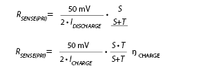
The turns ratio of the flyback transformer is selected based on the number of cells across the secondary winding and the maximum reflected voltage on the primary side and secondary side NMOS switches. For a 12-cell secondary, a 1:2 turns ratio from primary to secondary provides a good balance between transfer efficiency and voltage stress on the two NMOS switches. For a larger number of cells across the secondary, a higher turns ratio can be selected and still provide high transfer efficiency and manageable voltage stress on the NMOS switches.
Once the current sensing resistors and transformer turns ratio are defined, the primary inductance of the flyback transformer is determined. To do so, the operation frequency needs to be defined. The operating frequency is a function of the cell voltage, the current sensing resistor, the inductance of the primary, the number of cells within the stack, and the turns ratio of the transformer.
The operating frequency is generally set to approximately 150 kHz to reduce interference with other circuitry that may be in the system and to yield reasonable circuit component sizes with high transfer efficiency.
The nominal cell voltage is used in this calculation:
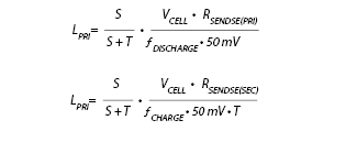
In most designs the average charge and discharge currents are set to be equal, which necessitates RSENSE(SEC) = RSENSE(PRI) · T. As a result, the charge and discharge frequencies are equal. Note that the frequency of operation is a linear function of the cell voltage: a 10% shift in cell voltage results in a 10% shift in the operating frequency.
Selection of the NMOS switches is determined by the peak balancing current and the drain-to-source off-state voltage. The drain-to-source off-state voltage can be estimated using the following expressions:
Good design practice recommends that the MOSFET breakdown rating be 20% higher than this minimum calculated value to account for voltage spikes due to leakage inductance ringing.
Some applications may require a series resistor capacitor snubber in parallel with the drain and source of the NMOS switch to reduce the ringing. These snubber circuits may lower the transfer efficiency but keep the NMOS devices within their safe operating region.
Additional NMOS parameters that need to be considered are the total gate charge (QG) and RDS(ON). The product of total gate charge and the operating frequency determines the gate current requirements for the primary and secondary gate drivers.
The primary gate drive for cells 1 to 5 is sourced from the cell above the selected cell. Cell 6 primary gate drive is sourced from the boost circuitry, which gets its energy from C6. All six secondary gate drivers are sourced from the VREG circuitry.
When all six balancers are operating, the secondary gate drivers present a load current on VREG of:
IV(REG) = 6 · QG · ƒ
resulting in a power dissipation of:
PPRI(DRIVE) = (VC6 - VREG) · IV(REG)
The primary gate drivers generate power dissipation in the LTC3300-1 of:
PPRI(DRIVE) = 2 · VCELL · QG · ƒ
The individual primary and secondary gate drive currents should be limited to less than 4 mA.
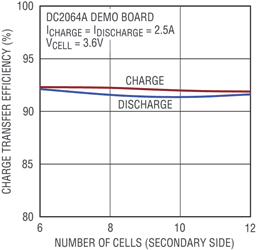
Figure 4 shows typical charge mode waveforms for a 2,5 A cell balancer with a secondary of 12 cells and a transformer turns ratio of 1:2. The primary inductance is 3 μH, RSENSE(PRI) is 8 m, RSENSE(SEC) is 16 m and the cell voltage is 3,6 V. Figure 5 shows the same cell balancer in discharge mode. Figure 6 shows the cell balancer efficiency for various numbers of cells connected to the secondary.
Interleaving secondaries in an 18-cell configuration
Large strings of cells can be accommodated by the LTC3300-1 by interleaving their secondary windings. Figure 7 shows an 18-cell stack with three LTC3300-1 ICs connected in series via the SPI-compatible serial interface.
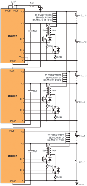
The transformer secondaries of the bottom LTC3300-1 are connected across (cell 1)- and (cell 12)+ while secondaries of the middle LTC3300-1 are connected across (cell 6)+ and (cell 18)+. The secondaries of the top LTC3300-1 are connected across six cells, (cell 12)+ and (cell 18)+.
The lower two devices have their BOOST and TOS pins tied to their respective V- pin and BOOST+ pins connected to the cell above the cell connected to their respective C6 pins. The top LTC3300-1 has its BOOST and TOS pins tied to the VREG pin.
A flying capacitor is connected between the BOOST- and BOOST+ pins along with a series 6,8 Ω resistor and diode connected from the BOOST+ pin to cell 6. The VMODE pin of the bottom LTC3300-1 is tied to its VREG pin while all other devices have their VMODE pins tied to their respective V- pins.
For more information contact Kevin Godfrey, Arrow Altech Distribution, +27 (0)11 923 9600, [email protected], www.arrow.altech.co.za
| Tel: | +27 11 923 9600 |
| Email: | [email protected] |
| www: | www.altronarrow.com |
| Articles: | More information and articles about Altron Arrow |


© Technews Publishing (Pty) Ltd | All Rights Reserved
 printer friendly version