


Over the years, I²C communication has become a recurring theme in customers’ questions about accurate real-time clocks (RTCs).
This includes basic subjects such as circuit setup and operation, and managing communications to all devices on the I&$178;C port.
In many instances, several key decisions need to be made prior to implementing circuit and firmware designs. This article provides a basic operational overview of the characteristics of the accurate RTC, so hardware/firmware engineers can decide how to effectively manage accurate RTC resources.
Key operational characteristics of the I²C port in accurate RTCs
Maxim’s accurate RTCs have dual power supplies. As shown in Figure 1, three power supply configurations can be implemented, depending on the application and desired use condition. The intent of these supplies is to offer managed, low-current power switching between primary power sources, and backup power sources such as batteries or supercapacitors.
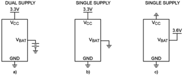
Unlike many standard RTCs that use dual-supply architectures, Maxim’s RTCs make I²C port communication possible, regardless of which supply is powering the device. This means that a user can communicate with the device when powered from the primary power supply or when the device is powered via the VBAT (or secondary supply terminal).
Most dual-supply modes only allow communication with the device when it is powered via the primary supply or VCC. This feature can complicate the design. Implementing a circuit that communicates regardless of the power supply used requires careful consideration of how to set up the I²C port. In the absence of a supply, the I²C port needs to be powered and available.
SDA and SCL should not be pulled to ground by the absent supply; otherwise communication cannot take place. The general approach when using two supplies is to use an ORing diode to switch between supplies. Figure 2 illustrates the technique described.
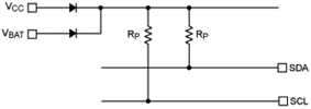
The importance of this method is to ensure that proper power supply isolation is achieved when one supply is not available or may be at ground potential.
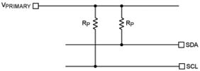
Figure 3 provides an example of the single-supply modes of operation, which are easily configurable for I²C communications. Pullup resistors are simply tied to the power supply that will be used during communications with the RTC.
Power supply-dependent device initialisations
Accurate RTCs will initiate certain actions that depend on which one of the two supplies is connected during an initial application of power. In applications where a battery is used (connected to VBAT), generally the battery voltage will be the first voltage that the RTC will see.
To conserve battery power, the RTC has a ‘freshness seal’ mode. This mode prevents internal circuits from powering before the beginning of full operation, and is released given that one of two conditions is achieved. First, an RTC will exit freshness seal mode when a valid voltage is applied to the VCC terminal. The second condition will occur if a valid I²C address is received by the device when operating from a valid VBAT supply voltage.
Once either condition is satisfied, the accurate RTC oscillator will start. The typical oscillator startup time is less than 1 second. Approximately 2 seconds after a valid VCC or valid I²C address, the RTC will make a temperature measurement and apply the calculated correction to the oscillator. At this point, the RTC will continue to run and make adjustments to frequency output as long as a valid power source is available (VCC or VBAT).
Temperature measurements will be made at regular intervals (specified by the device type) and calculated corrections will be made based on the oscillator time base – either digital (DS3231M, DS3232M) or analog (capacitive loading: DS3231S, DS3232, DS3234, DS32kHz).
On the first power-up (when an internal power-on reset (POR) sequence is initiated), the time and date registers are set to 01/01/00 01 00:00:00 [DD/MM/YY DOW HH:MM:SS] (where DD = day, MM = month, YY = year, DOW = day of week, HH= hour, MM = minute, SS = seconds).
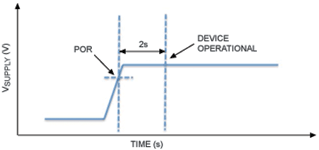
Communication with the I²C should be held off at least for the first 2 seconds after a valid power source has been established. It is during the first 2 seconds after power is established that the accurate RTC starts its oscillator, recalls calibration codes, initiates a temperature sensor read, and applies a frequency correction.
Attempting to read the device during a power-up can cause undetermined results with regards to timekeeping accuracy, or it may corrupt recalls in calibration memory. For crystal-based RTCs, a corruption in the recall event may result in the need to initiate another temperature conversion/frequency correction.
Most application problems with regards to I²C communication are related to I²C port activity being staged within the first 2 seconds of power being applied or the device receiving a valid I²C address when powered from VBAT.
Figure 4 illustrates a preferred timing diagram for safely beginning communication with an accurate RTC. Once the ‘device operational’ region is reached, I²C communication can safely begin without interrupting the POR initialisation sequences.
Managing power supplies in single-supply operation
Although Maxim’s accurate RTCs are designed to manage dual-supply modes of operation, some users desire to create custom dual-supply modes of operation external to the RTC. They choose to operate the RTC in a single-supply configuration, either applying power to the VCC terminal or VBAT terminal.
When designing custom external switching of supplies, careful consideration should be given to I²C communication and power supply decoupling. Also, when using a battery as a power source, one should consider decoupling requirements as they relate to power consumption.
It is important to understand switching characteristics such as noise, ground bounce and switchover times directly at the accurate RTC. Device power-initialisation sequences, frequency update rates and operational characteristics should be paid careful attention when in a single-supply mode.
Each device may have slightly different operational performance, depending on whether it is powered from the VCC or VBAT terminal. Micro-electromechanical systems (MEMS)-based RTCs will have different frequency adjustment rates, depending on whether they are powered from VCC (1 s) or VBAT (10 s).
Data sheet recommendations for decoupling capacitors on VCC are 0,1 μF and 1,0 μF. These capacitors are to be placed as close to the device as possible. In configurations where the user intends to switch supplies through the use of diodes or to place resistors in series with the power supply terminals, it is still recommended that decoupling take place as close as possible to the supply terminal of the device.
This is true regardless of whether the VCC or VBAT terminal is used as the primary supply. Figure 5 illustrates this position with a series resistor shown.
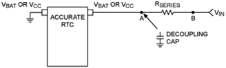
The configuration shown in Figure 5 is commonly found in applications where customers have experienced frequency accuracy issues. Customers who experience frequency issues place the decoupling capacitor at point B, which is not recommended. For best performance, it is recommended that point A be used as the decoupling point. This helps mitigate potential power supply pushing that results from current fluctuations due to basic device operational characteristics.
The general design rule is to not have any component other than the accurate RTC inside the decoupling capacitor position. Decoupling at point A provides the best option for noise reduction and improved frequency stability/accuracy performance of the accurate RTC.
Managing power supplies in dual-supply operation
Dual power supply operation with the use of a battery (on VBAT) to sustain clock registers and/or non-volatile device memory can benefit from two basic design approaches. First, the decoupling of the primary supply, VCC, should follow the recommendations presented in the previous section. Secondly, if the VBAT supply is truly a battery, a decoupling capacitor is not always needed or recommended.
Since decoupling capacitors placed across a battery will increase leakage currents, to achieve the smallest current consumption, no decoupling capacitor should be used. This is even more important if communication with the accurate RTC is not intended while the device is operating from the VBAT supply.
Conclusion
Understanding how a specific device operates from each of the three power supply configurations will help determine which configuration will best fit a particular application. Decoupling of the power supply will always be important to device performance, and following the guidelines outlined above will provide the best results.
Designers should always review circuit implementations to understand switching characteristics such as noise, ground bounce and switchover times at the accurate RTC with the intent of minimising these effects. Attention must be paid to the device power-initialisation sequences, frequency update rates and operational characteristics when in a single-supply mode. For all modes of power-up, a 2-second delay prior to initiating an I²C communication should be observed.
For more information contact Robin Scholes, Avnet Kopp, +27 (0)11 319 8600, [email protected], www.avnet.co.za


© Technews Publishing (Pty) Ltd | All Rights Reserved
 printer friendly version