


SiC (silicon carbide) power devices are enabling components, mainly in the context of higher switching frequencies and/or small footprints in power electronics.
However, this trend imposes new challenges on the packaging of the chips. Typical stray elements like inductances become crucial elements in the circuit. In addition, different considerations regarding the thermal design in power modules arise when SiC chips are taken into consideration.
Furthermore, the aspects of power density as well as the general utilisation of SiC’s high temperature capability are important factors in reliable implementation of SiC-based power semiconductors in modern systems. This article provides insight into how these boundary conditions can be implemented in innovative solutions using SiC chips.
Introduction
SiC power technology, predominantly in the form of Schottky diodes, is established in the market. High-power solutions using power module technologies have recently become available. Usually, the aim of such components is to enable system benefits, for example by increasing switching frequency or reducing losses. If this is successful, the high cost of SiC-based components can be compensated by reduced efforts for passive elements and/or cooling.
While discrete, unipolar SiC devices in the form of single chips are more or less ready to achieve higher frequencies (eg, >100 kHz in power factor control units), this is still a challenge for power modules. Solutions in a power range with traditional modules have high stray inductances and thus the di/dt is increased if combined with an increase in the frequency.
A plug-and-play between SiC and silicon at chip level in existing modules could devaluate the theoretical SiC performance. It is necessary to improve high-current modules in order to get the full benefit of SiC in the frequency range above 20 kHz.
Whilst the reduction of parasitic elements in power modules using SiC chips is in line with the approach used for future silicon solutions, it might happen that different optimisation criteria will apply for the thermal design. The reason for this is that the cost contribution of chips in a power module with SiC is different from one with silicon. Thus, the best solution for a given frame size with respect to semiconductor area placed in the module could be different.
Furthermore, it is expected that the die size of an SiC transistor at 1200 V, for example, comes down to one tenth or less of the area needed in the current silicon-based IGBT technology, assuming the same total losses for both options. This will result in a huge increase in power and current density, and will require more efforts with respect to effective heat removal and connection of chips to terminals.
Current and power density considerations
SiC Schottky diodes: Several new generations have been introduced since the first launch in 2001, each leading to a further increase in power density. Since 2006, Infineon has been using a merged-pin-Schottky (MPS) structure for 600/650 V diodes, mainly in order to offer sufficient surge current capability.
Other devices on the market are designed as JBS (junction barrier Schottky) diodes; from a design point of view, the layout is similar, the difference being that the main purpose of a JBS is to shield the electric field in reverse mode from the Schottky interface in order to keep the leakage current low, while in an MPS the main purpose is to withstand surge current.
In these diodes, only a part of the active area is used for current flow; the rest is passive, being in operation in the MPS for only a short period of time (pulse mode). This again represents a further local increase in the current density, as shown in Figure 1 using the basic principle of the MPS diode as an example.
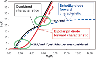
As shown, values today are close to the highest current densities for silicon power parts, which are known from low-voltage transistors (eg, 25 V at around 1300 A/cm²). Taking into account the voltage drop at operating temperature (which can be >2 V), it becomes obvious that heat generated by the power density at the chip with >2 kW/cm² can be effectively removed only if effective heat spreading is implemented between junction and case.
Another aspect of modern device design is the reduction of the die thickness. In the special case of vertical SiC devices, the active layer is just a few μm thick, and thus any additional material below it is merely an increase in the (differential) on-resistance and the thermal resistance of the chip.
It is thus reasonable to thin the wafers down to the smallest possible value, often defined by the handling capability in manufacturing. Infineon introduced thin (110 μm) wafer devices with its 5th diode generation (5G), offering a further step in power density, as shown in Figure 2.
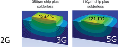
But this benefit has a drawback: the thermal capacitance, which is important under pulse current stress, is also reduced due to the shrunken volume of the semiconductor. Technologies must therefore be developed to compensate for this, otherwise only reduced pulse ratings are possible.
One approach is a good thermal connection of the chip to the lead frame, e.g. by Infineon’s solderless assembly technique, enabling the utilisation of the underlying copper as a support for pulsed operation.
SiC transistors: The focus today is on the implementation of unipolar high-voltage (600 V to 1700 V) transistors, offering threshold-free linear I-V characteristics, integrated body diodes, and negligible dynamic losses compared to the competing Si-IGBT technology.
The Ron x A values expected for 600 V components that seem to be achievable long term are around 1 mΩcm². The benchmark with the abovementioned low-voltage silicon technology shows that such values are still a factor of 20 higher than the best-in-class devices for 25 V today. So it seems that experience with silicon is sufficient to handle high current densities for SiC transistors.
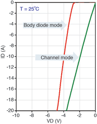
Nevertheless, one mode of operation will need closer attention. It seems to be mandatory for the success of SiC transistors in industrial applications to operate the internal body diode as a freewheeling diode. There might be some concerns regarding efficiency in this operation mode, because the forward voltage drop is too high; however, one can turn on the channel after a short dead time and then the I-V characteristic in reverse mode is identical to or even slightly better than in forward mode (see Figure 3).
In any case, there might be a critical situation should the driver circuit fail when diode mode is required by the system. To cope with this mode, one may be forced to define the actual current rating, not from the attractive threshold-less forward I-V, but out of the power handling capability in reverse mode. Thus, lowest VF is required, or alternative solutions for designing the diode function in the 3rd quadrant mode must be developed.
High-frequency optimisation
Real power circuits with SiC chips inside contain inductance and capacitance as major parasitic elements, and these cause serious deviations from perfect switching. Basic effects of parasitic inductance are:
* A voltage dip during turn-on of a transistor, caused by rise of current.
* A voltage spike during turn-off of a transistor, caused by current fall.
* The parasitic capacitance together with the inductance form resonant circuits, which show damped oscillations after each switching transition.
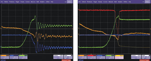
The effect of parasitics is already more pronounced when a combination of an IGBT with an SiC freewheeling diode is considered, since the diode performance also speeds up the transistor and thus, under improper conditions, oscillations could be observed as seen in Figure 4 (left side) when no special precautions are taken.
Therefore, an optimum circuit design with minimum parasitic inductance is a prerequisite for the optimisation of power semiconductors towards lowest losses. To meet these demands, rules were developed at Infineon for the design of power modules. It is well known that a strip-line type of circuit design brings parasitic inductance to a low value, depending on width and distance of the strip line.
The graph on the right in Figure 4 shows the effect on the switching performance of power semiconductors of an improved module layout, taking these considerations into account. Whereas, in the standard module, a severe over-voltage peak plus oscillations are observed, the new solution can eliminate these effects almost completely.
It has to be noted that the improvement was achieved without changing the chip technology, but simply by a more careful design of the package. These considerations will also take into account the fact that, on the midterm scale, paralleling of a high number of dies will be the preferred method of achieving higher power levels in SiC.
In order to avoid a degradation of the high performing SiC chips by an unsuitable environment, Infineon is committed to driving the implementation of SiC semiconductors only in module platforms that enable this approach.
Thermal considerations
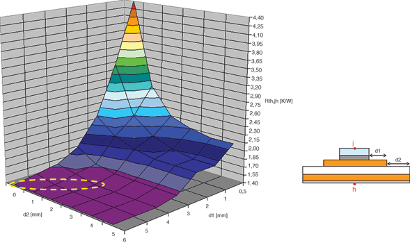
The final power handling capability of a semiconductor module is defined by the chip area inside the module combined with the thermal performance expressed by Rth. For silicon chips, as much chip area as possible is usually placed on a given footprint in a power module, because normally the area cost per chip is not so different from the cost per module area, mainly for larger power ratings.
In the case of SiC, different considerations apply. The chips are much more expensive than silicon ones, so it is beneficial to choose a different ratio of chip area to module area to get the optimum solution with respect to the price/power ratio for a given footprint. The reason for this is that, by proper design, the effective Rth per chip can be reduced by a factor of up to 4, due to heat spreading effects as shown in Figure 5 (baseplate-free module).
In addition, there is a trend towards higher maximum chip temperatures, in order to increase the removable heat for a given die area, and thus its current handling capability. It must be mentioned that doing this will increase the absolute losses, so that efficiency targets could be violated, depending on the ratio of loss increase to increase in power handling capability.
In contrast to IGBTs, this loss increase might be huge for unipolar SiC devices, because now a resistive component with a heavy increase in the Ron with temperature is in place, mostly with a power law in the form of Ron ~ TX, with x between 2 and 2,5, as recently presented for high-voltage SiC MOSFETs.
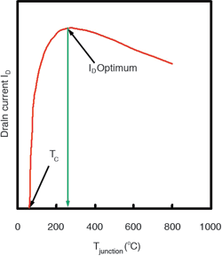
Taking this into account, one can see that, for unipolar devices, a continuous increase of Tj can even lead to a reduction in current handling capability, because more power is dissipated than can be removed by the increase of Tj. Figure 6 shows this result for a typical dataset, assuming x=2 as the exponent in the power law for the increase of the resistance with temperature.
In addition to these considerations, it is known that the reliability of power systems, mainly the power cycling capability, is degraded when the temperature swing between off state and maximum temperature is increased. Thus, for the sake of both efficiency and reliability, it might be wiser to offer good cooling and keep the temperature differences in the thermal stack low.
For more information contact Davis Moodley, Infineon Technologies, +27 (0)11 706 6099, www.infineon.com


© Technews Publishing (Pty) Ltd | All Rights Reserved
 printer friendly version