


Modern electronic assemblies are seeing an increase in the popularity of using conformal coatings to guarantee proper functioning under various climatic and environmental conditions. In particular in the areas of automotive, aviation and military, this is essentially important as aggressive environmental conditions may have an impact on an assembly’s performance.
These conformal coatings are categorised into three different classes:
• Class 1: general applications.
• Class 2: high reliability.
• Class 3: aerospace.
Their chemical compositions vary and typically consist of acrylic coatings (organic solvent), epoxy coatings (two-components), urethane coatings, silicones and UV-cured coatings.
First and foremost, conformal coatings provide electrical insulation for the assembly under all possible environment conditions. They serve to guarantee protection against moisture as well as chemical influences. Climatic changes, microbiological effects and pollutants also must not be allowed to affect an assembly’s mechanical or electronic properties.
Hence, the reliability of conformal coatings must be guaranteed to permanently ensure a printed circuit board’s (PCB) functionality under these conditions. But how can conformal coatings effectively and cost-efficiently be checked?
Conformal coatings and their inspection
Applying conformal coating is the last step within the PCB production cycle. Similar to the previous production stages, quality assurance measures must be executed. After coating the assembly, proper wetting is mostly visibly checked by manual means. Because manual optical inspection has proven inappropriate for high PCB output, so-called automated optical conformal coating inspection systems have been developed. They enable automatic testing of the correct wetting within the production line cycle.
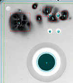
Before dealing with the function of an optical inspection system for conformal coating inspection in detail, it should be noted that there are transparent and non-transparent coatings. For transparent coatings it is mandatory they be fluorescent to assist camera evaluation. These fluorescent coatings are UV illuminated, emitting light in the blue range between 400 and 470 nm. Modern camera technology is able to capture this spectral range and take high-contrast images. Image processing technology may now differentiate between the fluorescent coating and dark PCB background. Consequently, a coating flaw is displayed as a dark spot.
In many cases, PCB manufacturers establish a coating plan defining which areas of a PCB conformal coating is to be applied to, and in which areas it must not be applied (forbidden areas). For example, coating should not be applied where the assembly is to be electrically contacted, as it would have an insulating effect impacting or disabling a PCB’s functionality. Additionally, there are positions on which coatings can but do not have to be applied (so-called ‘don’t care areas’).
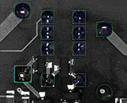
Particular drawing functions in the optical inspection system enable operators to define the test areas according to the coating plan. Now it is possible to define what can be rated as a coating error by means of a grey value threshold and the maximum defect size.
PCB warpage (vias) may generate false calls, also displayed as dark spots. They are filtered by a special algorithm and not evaluated as faults. Dark components or large boreholes may be wrongly indicated as coating errors as they are also displayed as large dark spots. To avoid misinterpretation, such areas are pre-defined in the inspection system as ‘don’t care areas’ not to be evaluated.
The coating’s flow characteristics must be considered in conformal coating inspection. As varnishings are not static before drying, contours at areas to be inspected may blur. Therefore the inspection area should be carefully selected in the image processing software. Additionally, small ‘ditches’ milled into the PCB around the area to be inspected should be included in the design. These hinder unwanted coating flow into non-coated areas.
Requirements for an inspection system
Fundamental elements of a modern optical test system are PCB-adapted pixel resolutions, the inspection system’s inline ability, flexible test program adjustments as well as special test functions due to coating presence or absence. Separately switchable LEDs in various colours such as white, red, green, blue or UV, a modular architecture for flexibility in terms of changing test tasks, or various camera variants and resolutions are indispensable requirements to execute safe and high-quality evaluation of conformal coatings.
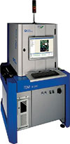
However, the inspection system’s functional area should not be limited to conformal coating evaluation or checking. Goepel Electronic’s TOM In-Line is an optical test system to inspect selective solder joints or displays. A wide range of practical test functions provides for numerous additional inspection tasks. Among others, powerful algorithms for component presence check, shorts inspection, colour detection or OCR are available.
A special benefit of this system is the combination of optical inspection with electrical test by means of JTAG/boundary scan to check an assembly’s correct functionality, producing benefits in terms of an increase in test and fault coverage. Uncoupled from the TOM In-Line apparatus and transport system, all single components such as camera, illumination and software can be integrated, specific to customer needs, into existing or new systems.
| Tel: | +27 11 869 0049 |
| Email: | [email protected] |
| www: | www.mykaytronics.co.za |
| Articles: | More information and articles about MyKay Tronics |


© Technews Publishing (Pty) Ltd | All Rights Reserved
 printer friendly version