


Much has been written about jitter and skew on Gigabit per second (Gbps) and faster differential signals that are traceable to the glass weave in PCB laminates. One solution that has been proposed is to route the signals in the PCB at an angle to the fibres in the glass weave to solve this problem. In fact, there is even one company that has applied for a patent on the concept of routing the signal traces at an angle to the weave of the glass fibres for this purpose.
Another solution proposed is to use a random distribution of glass fibres. Once the reason for the problem is understood, there is a much simpler solution.
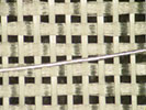
Figure 1 shows the glass weave of 1080 glass, a popular glass style for ‘high speed’ PCBs, along with a 3,5 mil wire to show how signal traces compare to the glass threads in the woven cloth.
As can be seen, the signal trace is quite small compared to the pitch of the threads in the weave (approximately 16 mil) and is small compared to the gaps between threads. It is easy to see that the trace could run over a thread for some distance and then between threads for some distance.
When the trace is over a thread it sees a dielectric constant of almost six and when it is between threads it sees a dielectric constant near three. This results in an impedance variation that is very large. It also results in a velocity change from about 12,7 cm per nanosecond to about 17,8 cm per nanosecond, respectively. If one member of a differential pair travels over a fibre while the other travels between fibres, their travel times would be quite different, resulting in significant skew.
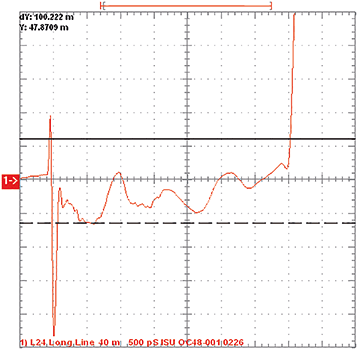
Figure 2 shows the impedance versus length for a 4 mil, 50 Ω trace travelling over 1080 glass cloth. The solid upper line and the dotted lower line are the ±10% limits around the 50 Ω centre line. Notice that the impedance has varied to minus 10% on one side and just barely gets over 50 Ω on the other side. This is a trace that remains on the same layer and has less than a 0,5 mil width variation. The variation is caused by the trace travelling on and off the glass fibres. Clearly, the velocity will vary in the same way, resulting in both excessive jitter and variations in delay between two members of a differential pair.
What can be done about this problem? Routing signals at a 45 degree angle would solve this problem but at the cost of very difficult PCB layout or difficult lamination changes to achieve the off-angle routing of signal traces.
The problem shown above is the result of uneven distribution of glass over the surface of the laminate. One way to solve the problem of uneven glass distribution would be to increase the density of threads in the weave from a pitch of 16 mil to something much tighter. The result would be a much more expensive glass cloth, along with a limitation on how thick the cloth could be because of the very small threads.
Perhaps there is another solution.
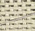
Figure 3 is a picture of 3313 glass cloth with the same 3,5 mil wire for comparison. The pitch of the threads is still approximately 16 mil as it is with 1080 glass. The difference is that the threads are flat, much like the webbing in a lawn chair. The result is a much more uniform distribution of glass across the surface. Notice that there are no gaps between threads. When viewed from the side, the glass distribution is quite uniform.
Figure 4 is a plot of impedance versus length for several 50 Ω traces travelling in both X and Y directions across a piece of laminate made from 3313 glass. Notice that the impedance is quite uniform along the length of each trace.
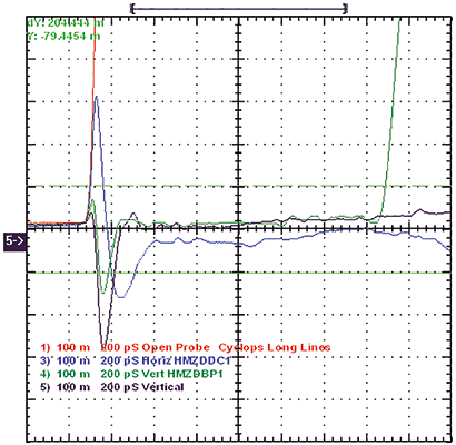
By simply changing the style of glass used in the laminate, the problems of varying impedance and velocity have been substantially reduced. Tests have shown that the jitter and skew problems encountered with 1080 and 106 glass styles have been reduced enough using 3313 glass that 10 Gbps differential signalling can be done successfully with resin systems such as ‘Hi Tg’ FR-4.
The author has fabricated dozens of PCB containing, multigigabit signals using this glass style with very good results. The 3313 glass style is not commonly offered by laminate suppliers, not because it is not readily available, but rather because it is not being requested. Perhaps it is time for laminate suppliers to add this weave as a standard offering.
Managing the tradeoff between PCB cost and signal quality at 10 Gbps
In another article, I covered how the choice of glass weave can influence the amount of jitter that is added to a high data rate signal by the PCB itself. In this article I will examine how the method used to route a 10 gigabit per second data signal can affect quality.
It is well known that the parasitic capacitance of the vias used to connect signals from integrated circuit and connector pins to traces in PCBs can adversely affect signal quality. As the data rate increases, this parasitic capacitance is often the limiting factor on how high the data rate can be driven in a conventional PCB.
At data rates of 10 Gbps, the capacitance of these plated through holes or vias is the primary factor limiting performance. One way to avoid this limitation is to route the entire signal trace on the top layer of the PCB connecting two IC pins without the use of vias or plated through holes. This is the most common technique currently in use for connections between the transceivers which connect the 10 Gbps logic devices and fibre optic cables. This method is doing a reasonable job, however it has several drawbacks.
The first of these drawbacks is that the impedance of traces on outer layers of PCBs is more difficult to control because of plating and etching irregularities and variations in the thickness of the prepreg that separates the surface layer from the underlying plane.
The second of these is that the most common surface finishes for PCBs that contain these traces is either electroplated gold over electroplated nickel or ENIG, both of which contain significant amounts of nickel. Nickel is a ferromagnetic metal; ferromagnetic metals react with the electromagnetic fields in these very fast signals in such a way that the signal loss is much higher than might be expected from an ordinary copper trace.
The third drawback is that space on the outer layers for signals is often blocked by the mounting pads of the components themselves, limiting the number of signals that can actually be routed on the top layer of the PCB. Users trying to connect multiple rows of SERDES (logic devices) to transceivers find it difficult, if not impossible, to make all of the connections on the top layer.
Figure 5 shows a method for solving the above problems. Instead of routing these signals on the top layer, laser-drilled blind vias are used to access layer 2 on which the signal traces are routed. This provides several benefits. The traces are etched on an inner layer where width and thickness control are more precise than on the outer layer.
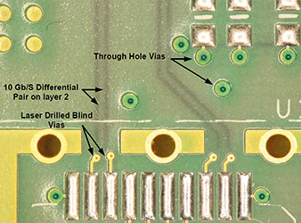
The primary dimension affecting impedance after trace width is the spacing to the nearest plane. In this case, the dielectric forming this dimension is laminate that can be selected with a well controlled thickness in advance of lamination. Since the traces are not on the top layer, they are not plated with nickel, so the ferromagnetic losses are avoided.
Since the traces are not on the top layer, it is possible to route more of them between SERDES and the transceivers, solving the congestion problem associated with multiple rows of transceivers on a PCB such as a switch or router product, with a high number of ports.
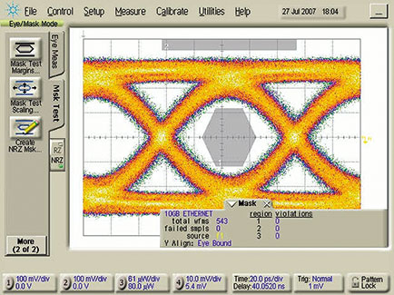
Figure 6 is the eye diagram for a 10 Gbps signal as it arrives at the receiver after having travelled 12,7 cm on a trace routed as shown in Figure 5 using the 3313 glass weave as a dielectric. What can be seen is that the signal has very low jitter and the eye is well defined. The only penalty associated with using this method is the need to add a laser drilling step to the process.
It should be noted that the blind vias are not drilled in the mounting pads of the devices. Instead, short ‘dog bones’ are added and the blind vias are drilled in a small pad outside the device mounting pads. The reason for doing this is to avoid trapping a small gas bubble under the ball when soldering is done (this is known to weaken the solder connection to a BGA ball).
About the author

Lee Ritchey has more than four decades of experience designing high-speed PCBs for supercomputers and high-performance Internet products. He now consults and gives training on his area of expertise, and has published a book on the subject.
Ritchey has partnered with EDA Technologies to come to South Africa to present his in-depth technical courses on designing and fabricating high-speed printed circuit boards. The 3-day courses will take place in Centurion, Pretoria from 1 to 4 March 2016, and in Stellenbosch, Cape Town from 7 to 10 March. Readers interested in attending can contact EDA Technologies at [email protected] or on +27 (0)12 665 0375.
| Tel: | +27 12 665 0375 |
| Email: | [email protected] |
| www: | www.edatech.co.za |
| Articles: | More information and articles about EDA Technologies |


© Technews Publishing (Pty) Ltd | All Rights Reserved
 printer friendly version