Breakthrough towards carbon nanotubes succeeding silicon
10 August 2016
Editor's Choice
News
Electronics Technology
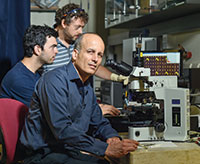
Researchers at the Technion-Israel Institute of Technology have developed a method for growing carbon nanotubes that could lead to the day when molecular electronics replace the ubiquitous silicon chip as the building block of electronics. The findings were recently published in the journal Nature Communications.
Carbon nanotubes (CNTs) have long fascinated scientists because of their unprecedented electrical, optical, thermal and mechanical properties, and their chemical sensitivity. But significant challenges remain before they can be implemented on a wide scale, including the need to produce them in specific locations on a smooth substrate, in conditions that will lead to the formation of a circuit around them.
Led by Prof. Yuval Yaish of the Viterbi Faculty of Electrical Engineering and the Zisapel Nanoelectronics Centre at the Technion, the researchers have developed a technology that addresses these challenges. Their breakthrough also makes it possible to study the dynamic properties of CNTs, including acceleration, resonance (vibration) and the transition from softness to hardness. The method could serve as an applicable platform for the integration of nanoelectronics with silicon technologies, and possibly even the replacement of these technologies in molecular electronics.
Professor Yuval Yaish.
“The CNT is an amazing and very strong building block with remarkable electrical, mechanical and optical properties,” said Prof. Yaish. “Some are conductors, and some are semiconductors, which is why they are considered a future replacement for silicon. But current methods for the production of CNTs are slow, costly and imprecise. As such, they generally cannot be implemented in industry.”
Due to the nanometre size of the CNTs (100 000 times smaller in diameter than the thickness of a human hair) it is extremely difficult to find or locate them at specific locations. Prof. Yaish, and graduate students Gilad Zeevi and Michael Shlafman, developed a simple, rapid, non-invasive and scalable technique that enables optical imaging of CNTs.
Instead of depending upon the CNT chemical properties to bind marker molecules, the researchers relied on the fact that the CNT is both a chemical and physical defect on the otherwise flat and uniform surface. It can serve as a seed for the nucleation and growth of small but optically visible nanocrystals, which can be seen and studied using a conventional optical microscope (CNTs, because of their small size, are too small to be seen in this way). Since the CNT surface is not used to bind the molecules, they can be removed completely after imaging, leaving the surface intact, and preserving the CNT’s electrical and mechanical properties.
“Our approach is the opposite of the norm,” Yaish continued. “We grow the CNTs directly, and with the aid of the organic crystals that coat them, we can see them under a microscope very quickly. Then image identification software finds and produces the device (transistor). This is the strategy. The goal is to integrate CNTs in an integrated circuit of miniaturised electronic components (mainly transistors) on a single chip (VLSI). These could one day serve as a replacement for silicon electronics.”
For more information visit www.ats.org
Further reading:
Compact direct Time-of-Flight 3D LiDAR module
Altron Arrow
Opto-Electronics Electronics Technology AI & ML
The VL53L9 from STMicroelectronics is the first direct Time-of-Flight (dToF) 3D LiDAR all-in-one module in ST’s portfolio, offering a resolution of 2,3K zones, wide field of view, on-chip processing, 100 frames per second, and sensing range from 5 centimeters to 9 meters.
Read more...
Solving South African power problems with locally built intelligence
Editor's Choice Power Electronics / Power Management
Smart metering infrastructure in South Africa remains patchy. The rollout has been slow, coverage is inconsistent, and for the most part, granular per-unit measurement simply does not exist.
Read more...
From the editor's desk: The art of measuring the truth
Technews Publishing
Editor's Choice News
All electronic measurements are a lie. The trick is making the lie as small as possible.
Read more...
Engineering for failure: why resilient telemetry matters more than perfect connectivity
Editor's Choice Telecoms, Datacoms, Wireless, IoT
One of the biggest assumptions in modern tracking systems is that connectivity will always be available. From an engineering perspective, this creates an interesting problem.
Read more...
Lesley Havenga: Building partnerships for Africa’s electronics future
Editor's Choice News
As Würth Electronik expands its footprint across South Africa and the broader sub-Saharan region, Havenga’s blend of manufacturing expertise, supply chain knowledge, and people-centred leadership appears well suited to the task.
Read more...
Generating negative voltages from a positive supply
Altron Arrow
Editor's Choice Passive Components
It is common for IoT devices, industrial sensors, meters, and medical equipment to require both a positive and negative voltage, and this article explains the options available to produce a negative rail from a positive rail supply.
Read more...
PEAK’s first automotive Ethernet solution
Industrial Data Xchange (IDX)
Editor's Choice Telecoms, Datacoms, Wireless, IoT
The PAE-Media Converter is a robust and compact device designed to connect Automotive Ethernet (100BASE-T1 or 1000BASE-T1) with standard Ethernet (100BASE-TX or 1000BASE-T) networks.
Read more...
What happens when trust can no longer live only in software?
Computer/Embedded Technology Electronics Technology
[Sponsored] For years, many enterprise security architectures treated hardware primarily as the execution layer, while software handled authentication, access control and trust decisions.
Read more...
EMC limits and levels
Altron Arrow
Editor's Choice Circuit & System Protection
As soon as electronics and electrical systems started interfering with each other, the world had to come to some consensus. Considering physics is universal and does not care about what country electrical/electronic products are used in, it should be the same everywhere, right? It is nearly there, but not quite.
Read more...
Sigfox SA powers smart connectivity
Editor's Choice Telecoms, Datacoms, Wireless, IoT
Sigfox South Africa is carving out a unique role, delivering low-power, wide-area network connectivity designed specifically for Internet of Things applications.
Read more...


 printer friendly version