


In our high-tech world, it’s easy to overlook the importance of the humble printed circuit board (PCB).
Buried in each electronic gadget or appliance there’s always at least one PCB and each one has to be perfect. There’s quite simply no latitude – a PCB fault will kill the device it’s part of.
Although they are largely passive platforms for surface mounted and leaded components, PCBs are by no means simple in design or easy to manufacture. Many of the fabrication processes have to be precisely controlled in case they destroy the board under construction or cause faults which will surface on the assembly line or in the field.
Now, to add to the challenges faced by PCB manufacturers, today’s already tiny PCBs are getting smaller and increasingly complex. The tolerances they have to work with are measured in microns and the faults they have to guard against are, quite literally, microscopic and buried deep within the layers of the board.
To check each layer as it’s completed, automatic optical inspection (AOI) and flying probe tests verify copper pattern quality and the integrity of pad, trace and via connections. Those tests are relatively straightforward, but checking the completed board, where the interior layers are entombed and the faults being checked for are microscopic and probably latent, is far more difficult.
Microsectioning is a commonly used technique as it can yield several levels of results.
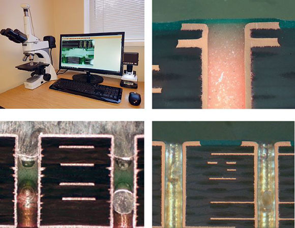
What is microsectioning?
To see inside a PCB, you need to take it apart. Microsectioning is a destructive testing technique. Several sample, or sacrificial, boards are taken from each fabrication run and a specific, pre-determined section is cut out for examination.
Samples are taken from the order overrun, so while the client is not losing any stock, he can match test results to specific production runs and so to specific batches of PCBs.
Potting, honing, polishing – preparing the microsection
The process of microsectioning involves selecting a specific section of the board the manufacturer knows will show signs of stress or defect, if there are any. The target segment is cut out, leaving a clearance to ensure the microsection to be examined is not damaged or distorted in the process. This segment is then potted in clear resin.
Once the resin has cured, the target zone – usually a cross-section along a line of vias – is exposed by honing and then polishing away excess material. Final polishing is done with 0,05 micron grit jeweller’s paste to ensure an optically correct, scratch-free surface.
This is a far more skilled and technical process than it seems from this brief description. As the microsections are going to be analysed using an electron microscope or powerful optical microscope, the surfaces have to be absolutely flat and scratch-free.
Faults found through microsectioning
Microsections are taken from various stages of the manufacturing run to ensure a comprehensive analysis of each batch of PCBs.
Generally, qualified inspection analysts will be checking or confirming the following:
• How the base material has held up through the manufacturing process.
• That the layers in a multi-layer board have bonded well.
• The plating thickness on the walls of plated through-holes or vias.
• That there is no tearing away of plating from via walls.
• The thickness of conductors.
• The thickness of surface finishes.
• Whether hole drilling has been carried out correctly and no damage has occurred through overheating or blunt drill bits.
• That the multilayer stack-up is met, relative to the design requirements.
• That copper wrap thickness and copper cap plating thickness are compliant.
• That there are no plating cracks, resin recessions, plating voids, delamination, smear, copper cracks, blistering, laminate void cracks, excessive wicking or plating nodules present.
The results of the microsection inspection are recorded on the inspection report and kept on file, together with the microsection sample, for at least two years. They can be referred to in the event of an inquiry into product failure or a query from the customer about the quality of any particular batch of PCBs
How often are samples taken?
The sample frequency depends on the size of the order – samples are taken whenever a predetermined square meterage of product has been processed. From each board sacrificed, samples are taken either from diagonally opposing corners, or as specified in the original manufacturing drawing.
If the PCBs are particularly complex and the order is small, the customer can include a test coupon into the design. The coupon will be a sample section of the PCB with the attributes of the PCBs being manufactured, but will not be a complete board. This saves the sacrifice of an actual PCB while giving the same results.
Production line health checks
Apart from quality control on PCBs, microsections reveal information the manufacturer will use for production line intelligence and health checks.
Apart from PCBs that are being made for clients, manufacturers run numerous test boards through their plants each day. These test boards go through the entire manufacturing process and are then used to check a multitude of factors including electroplating quality, laminate bonding, hole connection, drill quality, de-smearing and connection quality, to mention just a few.
Apart from pre-empting problems on their production lines, manufacturers use microsectioning in the search for perfection of their processes and techniques.
Designed for obscurity, checked for perfection
While PCBs are at the very core of our ability to make smaller and more reliable electronic equipment, you never hear about what brand of PCB is lurking in any device you may have in your tool kit at work or home.
PCBs are designed to remain obscure and put up with the worst possible conditions, particularly in the scientific, mining, automotive, military, avionics and aerospace industries. Their ruggedness and reliability are testament to the people who design, manufacture and test them, and to the processes and standards that have been developed to ensure their reliability and longevity.
| Tel: | +27 21 700 4900 |
| Email: | [email protected] |
| www: | www.cirtech-electronics.com |
| Articles: | More information and articles about Cirtech Electronics |


© Technews Publishing (Pty) Ltd | All Rights Reserved
 printer friendly version