


Field-programmable gate array (FPGA) technology has grown in popularity over recent years to a point where FPGAs are used in preference to ASICs in many applications. Gate arrays or ASICs of 50000 ASIC gates and below have been largely superseded by FPGAs. For higher gate-count designs, today's FPGAs can still be a compromise. Actel's new ProASIC PLUS family fills the gap between 50 000 and 300 000 ASIC gates, offering for the first time a true gate array alternative in a nonvolatile, In-System-Programmable FPGA.
Technology compromises
The lack of NRE charges coupled with the flexibility to buy and program devices as and when required, have always been big selling points for FPGAs. A few years back, FPGA logic densities lagged significantly behind those of ASICs, limiting their use as replacement devices. Now, many of today's FPGA offerings can easily accommodate designs in the 50 K-300 K ASIC gate sweet spot of the ASIC market. But FPGA device costs at densities over 50 K ASIC gates remain a problem; they tend to be considerably higher than equivalent gate arrays. There are also niggling issues surrounding FPGAs in terms of nonvolatility, security and ease of design.
The dominant programmable logic technology on the market is the SRAM-based FPGA. These chips have the great advantage of being reprogrammable and In-System-Programmable. But because of their complicated architectures they are rather inefficient in their use of silicon.
SRAM FPGAs are built around a complex logic block structure based on look-up-tables (LUTs) tied to flip-flops. The lines of interconnect, linking the logic blocks are programmed using SRAM-based switches. Each SRAM switching element typically comprises six transistors and there will be millions of these switches in a large device. Clearly, the switches constitute a substantial silicon overhead compared to a gate array with a similar logic capacity.
Moreover, because the SRAM FPGAs have a more complex, coarser-grained architecture than the two-input/one-output NAND structure of a gate array, achieving timing convergence is more time-consuming because designs do not map in a straightforward fashion. Timing closure can take many iterations, adding weeks in some cases to the expected design cycle.
Other sticking points surrounding the use of SRAM FPGAs include their nonvolatility (they are not 'live-on-power-up') and their requirement for an associated boot PROM to hold the circuit configuration. A boot device adds to the cost and complicates both system and board design compared to a single gate array. For applications such as line interface cards that need to be 'live-on-power-up', SRAM FPGAs have to be isolated with extra circuitry so that they appear 'live' during their boot-up process.
As the value of the designs implemented in FPGAs increases, security limitations of SRAM-based FPGAs are an area of concern for some users. They are worried that devices could be cloned by copying a bitstream sourced to the FPGA either by a nonvolatile boot PROM or a microprocessor.
Some of the above problems are addressed by antifuse technology. Antifuse FPGAs are high-speed, 'live-on-power-up' devices that are based on a fine-grained, ASIC-like four-input/one-output logic structure comprising NAND and NOR gates with an associated flip-flop. The antifuse programming switch uses a very silicon-efficient dielectric embedded within the metal layers 2 and 3 of the chip, thus taking up virtually no overhead compared to the SRAM switch. Interconnect lines are connected using a programming impulse to short out the antifuse dielectric.
Security-wise, the technology is hard to beat; determining the on-off state of an antifuse requires physically delving into the chip. The antifuse is less than 100 nm diameter and programmed fuses are not visible when viewed from the top of the die. Nevertheless, antifuse devices are one-time programmable and so do not offer the flexibility of reprogrammability and in-system-programming that many users require.
The best of both worlds
Ideally, users would like a technology that combines the best aspects of FPGAs with those of gate arrays. Flash-based devices, using Actel's ProASIC technology, are the first FPGAs that can offer the best of both these worlds. Like SRAM PLDs, ProASIC PLUS devices are reprogrammable, and In System Programmable. Like ASICs and antifuse FPGAs, they are single-chip devices and 'live-at-power-up'.
In physical terms, the Flash-based programming switch is seven times smaller than an SRAM switch making it inherently lower cost. The technology also uses only half of the power consumed by LUT-based programmable logic devices at the same supply voltage.
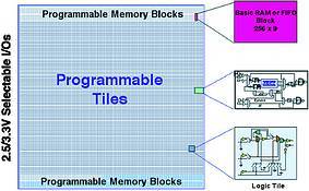
ProASIC PLUS, Actel's latest Flash family, offers for the first time, a single-chip, nonvolatile, in-system-programmable alternative to 50 K to 300 K-gate ASICs. With up to 1 million system gates, ProASIC PLUS devices target the sweet spot of the ASIC market and provide a cost effective, nonvolatile alternative to SRAM-based FPGAs. The family is built on a 0,22 µm, 4LM Flash-based CMOS process. The largest member of the family boasts 1 million system gates, 198 Kb of configurable 256x9 embedded RAM and 712 I/Os. The ProASIC PLUS chip layout is shown in the figure. The memory blocks, designed to fit telecommunications and networking applications, can be configured as single-port or dual-port memories with independent write and read clocks. Each memory block also includes FIFO control and parity logic.
On-chip features of the new family include analog clock conditioning functions providing two phase-locked-loops; a 1,5 to 250 MHz frequency range; multiple, divide and delay options; and phase shifts of 90, 180 and 260°. I/Os will handle 50 MHz PCI and include two high speed LVPECL differential pairs (clock or data inputs). The I/Os have been designed for easy in-system-programmability via either a microprocessor or an on-board adapter.
Security-wise, Flash-based FPGAs are as impenetrable as antifuse devices. There is no configuration bitstream and as single floating gates are simply charged or discharged to set the state of the programming switches, there is nothing to detect by any material analysis. In addition, a read-back security bit prevents programming content from being read from the device. A key, inserted during manufacturing, locks the silicon to the design.
ProASIC PLUS architecture
At the heart of the basic ProASIC PLUS architecture is a fine-grained sea of programmable three-input/one-output logic cells. These are functionally similar to the two-input/one-output ASIC logic cell. The ProASIC PLUS cells, called 'tiles', can implement almost any function of three inputs, as well as flip-flops and latches. As a result, ProASIC PLUS designs can achieve over 90% device utilisation, regardless of the mix between sequential and combinatorial logic.
The ProASIC PLUS cell comprises around nine gates - considerably smaller than the 100 or so gates that make up the logic blocks in an SRAM FPGA. One potential drawback to using such a fine-grained structure is that many more switches are needed to carry out the same function in ProASIC PLUS cells. However, being Flash-based, the ProASIC PLUS switches use just two transistors rather than the six typically required to build an SRAM switch. The small Flash switch size means there is room to implement many more switches without sacrificing extra die area. A high-speed routing hierarchy connects the tiles together. As the routing network has almost double the number of programmable switches as SRAM devices, place and route times are faster and device utilisation much higher.
For the FPGA design environment, Actel offers its next-generation Libero2.0 suite. Libero integrates industry-leading design tools and streamlines the design flow; manages all design, run and report files; and passes necessary design data between tools. Libero includes Innoveda's ViewDraw schematic capture tool; SynaptiCAD's WaveFormer Lite test bench generation system; Model Technology's ModelSim simulation and design verification software; Synplicity's Synplify synthesis software; and Actel's Designer Series place-and-route software and Silicon Explorer verification and logic analyser tool.
For ProASIC PLUS designs that go to very high volumes, the ASIC-like architecture of the technology enables a straightforward path to standard cell ASIC. Actel offers a conversion programme based on a 0,22 µm process for converting the FPGAs to lower cost standard-cell equivalent devices.
For further information contact Kobus van Rooyen, ASIC Design Services, 011 315 8316, [email protected]
| Tel: | +27 11 315 8316 |
| Fax: | +27 11 315 1711 |
| Email: | [email protected] |
| www: | www.asic.co.za |
| Articles: | More information and articles about ASIC Design Services |


© Technews Publishing (Pty) Ltd | All Rights Reserved
 printer friendly version