


It is trite to speak of smaller, faster, cheaper, better. Each is a given in today's electronics manufacturing environment. If anything, the current downturn has accelerated miniaturisation and further pushed everyone everywhere into deep cost reductions. Doing more with less, another industry mantra, is no longer a goal to be achieved someday - it is a necessity to be accomplished now...or if truth be told, yesterday.
Given these undeniable industry drivers, it is not difficult to see that the equipment and processes electronics manufacturers use must evolve to meet the above critical drivers. And part of the evolution will include more functional, smaller profile, smaller footprint components. That is why land grid arrays (LGAs) or leadless lead frame packages (LLPs) and chip scale packages (CSPs) are 'suddenly' so popular. In mobile phones, PDAs and digital cameras, these are the packages of choice - not only for their size and functionality, but also for their low manufacturing cost.
In particular, CSPs have the speed, density and manufacturability that OEMs and contract electronics manufacturers (CEMs) require. Moreover, since they can be placed using today's standard SMT processes and machinery, CSPs allow designers and manufacturers to do more with less.
Rework just will not go away
It is ironic in some ways: electronics manufacturers are more automated than ever; placement machines, ovens, dispensers, etc, can all work at breakneck speeds. Logically, then, it would seem the need for rework should decline. It has not. In fact, just the opposite: higher density assemblies with more solder joints and smaller packages inevitably lead to increased levels of rework. More solder joints means there are more chances for defects - and more, not less rework.
The face of rework itself has changed. Once the 'hidden secret' of CEMs and OEMs, and long considered a profit-draining process, successfully reworking an expensive assembly (thus saving both production time and materials) is often a critical key to long- and short-term profitability. In this arena, CSPs excel. Unlike flip chips, many CSPs do not require underfill. If they have a flexible layer between the solder ball and the die, no underfill is needed. So, they can be more easily reworked - given the proper equipment and good operator training.
In theory, rework is rework - be it basic SMT components, advanced packages or 0201s. No matter, the steps are similar. The keys to effective CSP rework, however, can be found not in the similarities, but in the differences that can make or break successful rework, and in the essential tools needed to get the job done quickly and efficiently.
The basic steps required
The basic steps to the removal and replacement of CSPs are straightforward enough:
* Establish thermal profile.
* Remove failed component.
* Clean and prepare site.
* Replace component with flux or solder paste.
* Reflow.
* Inspect.
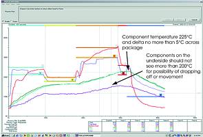
Naturally, convection rather than radiation is the heating method of choice. Using a soldering iron (conduction) is not an option. In addition, convection allows for tight process control, which is essential in establishing a good, repeatable thermal profile, that will not overheat the component, or hold for too long above reflow. Establishing the correct, ideal profile takes experience and patience, although the basic requirements for any profile are well understood.
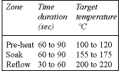
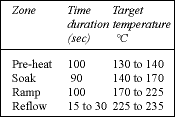
This process is particularly critical when working with lead-free assemblies. The higher temperatures needed for lead-free (up to 225°C) coupled with the thermal sensitivity of CSPs can be problematic without the ability to ramp temperatures at a rate that will not harm packages. The latest technology rework systems are more likely to use four heating zones and one cooling zone. Most older systems work with a more traditional three-zone model and no system for cooling down. The addition of a controllable pre-heater to a rework system helps meet future process demands, including lead-free. Efficient, controlled pre-heating avoids the thermal damage risked when working expensive but sensitive packages unsuitable for heating above 240°C with quick reflow times.
Some lead-free reflow profiles are as small as 15 seconds above specified reflow temperature. A typical lead-free profile is shown with peak temperatures around 223°C to 235°C and times as low as 15 s in the reflow zone. This means very good temperature controls and profile controls are essential.
To help protect packages from the increased heat of lead-free processes, independent top and bottom heater control is essential. In short, as lead-free alloys become mainstream, greater care must be taken to develop a thermal profile that can reflow the new alloys without damaging CSP/BGA/LLP packages.
Through closed-loop, time, temperature and airflow parameters, contemporary rework systems can help operators adapt to lead-free. In addition, and just as important, enhanced process control features guarantee repeatability, which is critical for companies with multiple locations in various parts of the world. Different voltages and frequencies affect performance of machines in many cases.
On any reflow soldering system that heats both sides of a PCB assembly, the required solder joint temperature is a function of how much heat is applied to both sides. And while it is possible to reach a specific solder joint temperature with a number of heat settings, the incorrect combination can lead to low yields and, in some cases, catastrophic results, including warping due to excess heat on the topside. This often causes bridges in the corners of BGA and CSP packages.
It is here that an experienced operator using equipment that allows for precise process control can play a paramount role in successful rework. If minimal warpage occurs, for example, a BGA lifted by just 0,1mm across the device, is enough to cause an open circuit. Even if the board/component survives this process with no apparent defect, the joint will be constantly under strain as the board returns to its normal shape, causing long term reliability problems. Eliminating warp generally involves creating a better balance between the bottom and top side of pre-heat temperatures. This is best achieved with full convection, as in the assembly line reflow ovens.
Convection and airflow
Convection systems employ either high or low airflow. For CSP rework, for instance, low airflow systems are preferred. As already stated, CSPs are normally found on high density PCBs. Space is at a premium and adjacent components can be easily reflowed and moved out of place during the rework process. High airflow systems increase the chances of moving adjacents - ruining alignment and creating more rework. Low airflow systems reduce the chance of shifting components, provided airflow levels are below 15 l/min and they feature a low velocity reflow nozzle design.
Once reflow is accomplished, component removal is generally accomplished with a vacuum pick-up. Care must be taken as excessive vacuum pressure can cause the solder to collapse and adhere to the PCB, making clean up slower and difficult.
Cleaning
Once the component has been removed and pad integrity has been checked, the site is then prepared for component reattachment.
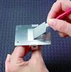
Removing residual solder using a soldering braid is still the preferred method, as braid allows the operator to achieve flat pads (which are preferred when solder paste is to be applied for re-attach). This process must be carried out in the case of leadless lead frame packages. If dome-shaped pads are preferred, for example, then only flux will be applied, and a wave solder tip is best for site cleaning. Of course, this process can only be used when pad geometry is uniform. Otherwise, solder joint heights will differ. When applicable, the method is a reliable and less damaging way to remove residual solder. Special solder tips called 'hoof tips' are available for this purpose.
In either case, to prevent thermal damage, and to speed the cleaning process by eliminating the need for constant setting and resetting of heating parameters, many rework facilities are moving away from 'traditional' soldering irons in favour of tools that automatically control tip temperature.
In general, any tool that increases process control, thus reducing operator variability and allowing for 'copy-exact' rework from facility to facility, is preferred. As the industry itself moves into China and other remote manufacturing sites, the need for transparent tools, those that can take the guesswork out of rework, will increase dramatically.
Material deposition - a new approach
When working with array packages, either flux (dip transfer method) or paste can be used for reattach. The device type and/or solderball composition will determine whether solder past or flux is used. In either case, operators must pay close attention to material deposition. How accurately the solder or flux is deposited will directly affect the yield and size of joint. With a conventional SMT component, for example, a defect in the rework can be easily rectified by retouching. With array packages, however, a single failed solder joint would necessitate starting the entire rework process from scratch.
With paste, for example, stencils are still being used to apply solder paste to the PCB itself, albeit with great difficulty and significantly reduced yields. This traditional method of paste deposition creates problems, as stencil flatness and position are troublesome, and there are concerns about access due to the close proximity of the adjacent components.
[New products like Metcal's Component Stenciling Templates bypass the time and cost required to perform the task using a stencil, and can increase user productivity by as much as 400-500%.]
Printing onto a PCB, when fully populated, is difficult due to size and packaging density around the devices. Today, small chip components are often very close to the packages. To alleviate this problem, a method of printing on the package has been developed. This solution prints the standard thickness of paste used in assembly, but onto the package. If this method is followed this will control the solder volume for replacement in the rework process.
Printing directly onto the component is a relatively easy process. A specially-designed plate is used to apply solder paste to the component with the same size and shape as originally done on an inline screen printer. The goal is to place approximately the same volume of paste as was originally deposited by an inline printer during the original manufacturing process.
The direct deposition process involves printing solder paste onto the component before it is picked up by the placement head. Not only is this new process simple, it is also quick to perform and can increase productivity up to four to five times in place of stencilling the PCB substrate. This is an ideal process for small components and situations where traditional stencil access is limited by the close proximity of adjacent components.
When working with LGAs, the component body outline is used to register the component to the stencil. Direct printing onto the component is especially useful with LGAs with different pad dimensions on the same component, as it allows operators to print different amounts of solder at a uniform height across the bottom of the device. It should be noted that on these devices flux and drag-solder pad cleaning methods cannot be used.
For packages with solderballs, the balls themselves can be used to align the stencil. With LGAs, however, there are no balls to locate on. In these cases, the stencil is made to help locate the component body by registering on the edge of the component itself.
Replacing the component
A split-optics vision system is necessary to help operators achieve higher process yields and better quality. The component is aligned, placed with the vacuum pick-up tube and reflowed with hot air or gas. The thermal profile developed for removing the component is again employed so that the new device is not damaged during re-attach. Adjusting the profile, however, may be necessary depending upon the type of flux or paste being used.
Automated placement features and better vision systems on newer rework systems help operators improve accuracy. X- and Y-axis control are standard and necessary - better machines incorporate Z-axis motorised control to help place components at the exact height required, without crushing the paste. Accuracies to 0,025 mm are ideal for precise, repeatable CSP placement and LLP placement.
Inspection
With leaded components, it is a simple matter to look for good solder joints and the absence of shorts, using a low magnification inspection system. With CSPs and other array packages, inspecting the integrity of solderballs (size, positioning, bump geometry, etc) requires either X-ray systems and/or optical inspection systems to see underneath the components.
X-ray inspection can highlight certain faults, such as voids, shorts, and bridging; however equally serious problems like component opens or joint cracking and partially soldered joints are not easily found. However, there are some things X-ray cannot detect - process-related problems like unsoldered joints, flux contamination and grainy joints.
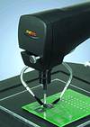
To detect these faults, optical inspection systems using an endoscopic-type mechanism are preferred. With advances in optics and improved software, latest technology optical inspection systems can catch 90% of errors - often eliminating the need for expensive and time-consuming X-ray. For those already using X-ray, an optical inspection system can be employed as an additional tool - as the first line of inspection, before assemblies are sent to X-ray.
However, there are a few requirements for effective optical inspection. Given today's high package densities, any inspection system must be able to manoeuvre between components - spaces as tight as 1,1 mm. Some endoscopic systems can perform in these tight spaces, others cannot. For complete optical inspection, systems need to be able to 'see' under array packages with low standoff heights, down to 0,05 mm for micro-SMD as an example.
Metcal's new optical inspection system requires just a 1,1 mm distance between components to achieve optimum inspection.
A final caveat: underneath the typical BGA or CSP there resides a large number of solder joints and 100% inspection may not be practical or cost effective. Both optical inspection and X-ray methods are, however, essential tools in good process development.
Conclusion
CSPs, LLPs and other array packages continue to gain in popularity, as devices get smaller, cheaper and more complex. And in spite of automation, rework remains an integral part of successful electronics manufacturing. Reworking array packages, in particular CSPs, is challenging - particularly in light of industry trends that include higher board densities, far-flung manufacturing sites, the need for repeatable process control, and lower paid wage workers who ultimately perform the rework process.
Reworking CSPs is, in many ways, not very different from standard SMT devices. Effective rework demands adapting existing processes to the realities of hidden solder joints and temperature sensitive components. Equipment, too, must evolve. Better vision, more accurate temperature profiling, more accurate placement and process repeatability must become standard in every rework system. It is not 'if' we will need to consider these new packages, it is 'when.'
For more information: John Watson, Test & Rework Solutions, 011 708 3451, [email protected]
| Tel: | +27 11 704 6677 |
| Email: | [email protected] |
| www: | www.testandrework.co.za |
| Articles: | More information and articles about Test & Rework Solutions |


© Technews Publishing (Pty) Ltd | All Rights Reserved
 printer friendly version