


This article describes how to use event-driven techniques to maintain the lowest possible power consumption in single-cell, battery-powered intelligent sensor applications. Examples of such applications are detectors of glass breakage, sound level, fire, and smoke. These same applications include a microcontroller to control the system and a high-resolution, analog-to-digital converter (ADC) to search periodically for interesting realtime sensor output signals.
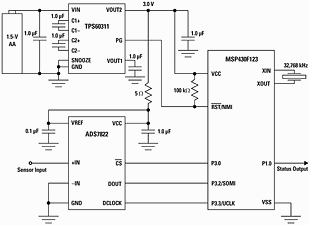
To extend battery life, system power consumption must be managed to the absolute lowest possible level. To reduce power consumption, intuition points to a slowly-operating data acquisition solution. On the surface this intuitive approach seems reasonable; but it is misleading, especially when analog circuitry is involved. Although power consumption does typically scale with conversion rate, it will be demonstrated that extending system time in standby modes is the largest contributor to total power reduction. Activity must occur as fast as possible in short 'bursts', allowing the system to return quickly to a standby mode. A micropower intelligent sensor system using the MSP430F123 Flash MCU, ADS7822 12-bit ADC, and a single-cell TPS60311 DC-DC boost converter is examined. The entire system is powered from a common 1,5 V AA battery. See Figure 1.
Enabling single-cell, 3-year battery life
The example examined is powered from a single 1,5 V AA alkaline battery with a typical usable energy value of 1000 mAh. If the application has a targeted 3-year battery life, total current consumption must be managed as follows: 1000 mAh/3 years/365 days/24 hours = 38,0 µA.
The example presented also assumes that the sensor must be sampled at a 2 ms interval (512 samples per second) to acquire the necessary realtime data to detect an event such as glass breakage.
Serial interface
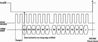
The interface between the MSP430F123 MCU and ADS7822 ADC is glueless. The MCU's integrated USART peripheral is used in SPI master mode to drive communication with the ADC. The USART clock (UCLK) is provided to the ADC (DCLOCK), and receives data on the slave out master (SOMI) from the ADC digital output DOUT. In the example, software uses port pin P3.0 to control the ADC chip select (CS). Any available port pin can be used. With CS and software, the MCU directly enables and disables the ADC. The ADS7822 provides 15 bits of data: 2 bits for sampling, 1 null bit, and 12 bits of conversion code. Typically, SPI serial communication exchanges data as 8-bit bytes. To transfer the 15 bits from ADS7822 to the MSP430, two 8-bit transfers are made back-to-back and packed into a single 16-bit word by using software. The word data is rotated right to eliminate the erroneous extra bit and is then AND'ed with 0FFFh to expose only the interesting 12 bits of ADC conversion code. The result is right-justified.
The MCU enables the ADC by resetting CS. The conversion is started and timed with 16 bits of data exchanged by writing two dummy bytes back-to-back to the USART transmit buffer (TXBUF). TXBUF is double buffered, so back-to-back 8-bit writes will transfer a total of 16 bits. Though no data is actually transmitted from the MCU, writing to TXBUF automatically initiates a complete bidirectional SPI transfer, including UCLK generation that is required by the ADC DCLOCK. The data transmit function of the USART is simply ignored. After the first 8-bit byte of data is received from the ADC into the USART shift register, it is transferred automatically to the receive buffer (RXBUF). The second byte of data is automatically received next as software is recovering the first byte from RXBUF. The second byte of data is recovered; then the 16-bit result is packed into register R15. See Figure 2.
Slow operating system analysis
First consider the intuitive approach to saving power; that is, simply clock the entire system slowly from the available 32 kHz watch crystal. With the MSP430 CPU master clock (MCLK) clocked continuously at 32 kHz, current consumption is approximately 10-12 µA. With this slow clocking, the MCU will be essentially 100% active in order to complete the required sample and decision loop at the 2 ms interval. No standby modes are possible. The SPI UCLK at 16 384 Hz (32 768/2) can conveniently clock the ADC DCLOCK. With 16 clocks per sample, the ADC can complete a conversion in approximately 1 ms, leaving 1 ms for power-down and time for the MCU to complete the calculation. The active current of the ADS7822 is approximately 200 µA. Powered-down, the ADC current consumption is a negligible 50 nA. The MCU will be 100% active, and the ADC 50% active.
In snooze mode, quiescent current of the TPS60311 DC-DC charge pump is 2,0 µA typical and can deliver 2 mA to the system. Since the system should never use more than 2 mA, and the 2 µA TPS60311 snooze current will be a constant draw, snooze should be the only mode ever used.
With slow (32 kHz) processing, the system consumes an average current as calculated:
IBAT = MCU + ADC + DC-to-DC
= (10 µA x 1,00) + (200 µA x 0,50) + (2 µA)
= 10 µA + 100 µA + 2 µA
= 112 µA.
At an average current consumption of 112 µA, the system exceeds the 38 µA maximum for 3-year, single-cell battery life. The most significant current consumption is the 50% active duty cycle for the ADC. The analog circuitry of the ADC is the prime current consumer and is largely unaffected by speed of conversion. The ADC's total current consumption is approximately 200 µA and is almost unchanged over the full DCLOCK range of operation at 10 kHz-1,2 MHz. With this in mind, it makes sense to convert as fast as possible and spend as much time as possible in power down. With a slow 32 kHz MCLK, the MCU is 100% active; no standby mode is possible and no processing bandwidth available for increased digital signal processing or additional sensor sampling.
Burst mode system analysis
Next consider a burst technique - fast, short active-mode intervals with extended system time in standby. The MSP430 is clocked by a single 32 kHz watch crystal that drives an internal auxiliary clock (ACLK). The ACLK is used in the example to drive only the watchdog timer (WDT), configured by software as a 2 ms interval timer. As configured, the MCU operates normally in low-power mode 3 (LPM3) with only the ACLK and WDT interrupt active. At the programmed 2 ms interval, the WDT interrupts the system and activates the CPU, which is then driven by a high-speed MCLK clocked from the on-chip digitally controlled oscillator (DCO). It is important to note that the fast-starting DCO also allows the MCU to move from standby to high-speed active mode in less than 6 µs. The DCO has been configured by software to operate in the 1 MHz range. The sub-master clock (SMCLK) used by the USART has also been configured to clock from the DCO.
As defined by the programmed WDT interrupt interval, the ADC is sampled and a decision made every 2 ms. The ADC measurement and decision code requires approximately 70 active CPU MCLK clocks. At 512 measurements/ decisions per second, the CPU is active a total of 70 x 512 = 35 840 clocks per second. Assuming that the CPU is clocked at 1 MHz (1 µs per clock), the active duty cycle for the CPU is 35 840 / 1 000 000 = 3,5%. The MCU active current is approximately 300 µA. The standby mode LPM3 current is 1,6 µA and is dominant 96,5% of the application time. Using a 500 kHz DCLOCK (1 MHz/2), the system samples the ADS7822 512 times per second, with each sample taking 16 clocks. The ADC will be 1,6% active and 98,4% powered-down.
For maximum power conservation, the MCU manages the system such that MCU and ADC spend the vast majority of time in standby mode, with an average standby current consumption of all components ~ 3,6 µA.
With a burst-mode technique, the system consumes an average current as calculated:
IBAT = MCU + ADC + DC-to-DC
= (1,6 µA x 0,965 + 300 µA x 0,035) + (200 µA x 0,016) + (2,0 µA)
= 11,54 µA + 3,2 µA + 2 µA
= 17,2 µA.
With burst-mode programming, the system consumes an average current of only 17,2 µA and easily surpasses the target of 38,0 µA required for 3-year battery life. The additional power reserve can be used to compensate for other requirements such as faster sampling, sensor signal conditioning, or weak/leaky batteries. Also, the current budgeting does not take into account the power required to support the activity if a trigger event occurs - ie glass breakage or fire detection. It is thought that these events would be very rare and clearly the exception to normal operation.
Further reduction in power consumption
It has been demonstrated that managing the system active duty cycle is of utmost importance for reducing power consumption in intelligent sensing applications. The primary goal should be to minimise active time and maximise time in standby and power-down modes. MCU code execution should be fast and efficient. MCU activity should be event-driven and use interrupts that identify the code to be executed as fast as possible; ie avoid cyclewasting subroutine calls, polling, and bit-test skip chains. The watch crystal and DCO combination is ideal for battery-powered applications, providing both an ultra-low-power standby mode and a fast processor clock. The fact that the DCO can start and is stable in less than 6 µs provides very large power savings by reducing start-up time. The start-up time for a typical crystal or resonator is in the 10 ms range - time that would be wasted and consume significant power. Using the DCO can reduce standby-to-active wake-up time by over 1000 times.
The ADC must also be powered-down as long as possible. If more limited resolution data can be used, consider short cycling. That is, inspect only the first 8 bits of ADC conversion code (which represent the 5 MSB of the conversion) in the first of two SPI transfers required for a complete conversion. Determine if the first 5 bits are interesting; if not, terminate the second SPI transfer to power down the ADC.
In all cases, if a voltage regulator or step-up converter is used, reduce system VCC as much as possible. All components will use less power at a lower VCC.
The code is short, interrupt-driven, and programmed in assembler. This combination ensures that the MCU executes code as fast and effectively as possible with no power-wasting extra cycles.
The demonstration firmware is coded with a 'Mainloop' and single active WDT interrupt service routine (ISR). Three MSP430F123 USART pins on port 3 are used to interface with the ADS7822 ADC, and port 1 pin P1.0 is used as a status indicator. All MSP430 port pins default to the input direction. In a final application, unused pins should be configured to the output direction to avoid power-consuming floating inputs.
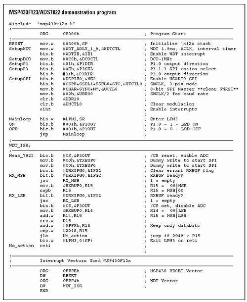
The code demonstration firmware first initialises the peripherals. Next, inside the Mainloop, setting the appropriate bits in the CPU status register (SR) forces the processor to enter LPM3:
Mainloop bis.w #LPM3,SR ; Enter LPM3
The CPU, DCO, and code execution halt at this point, but the pre-configured 2 ms WDT ISR is active with the timer clocked by the 32 kHz ACLK. It is at this point that the code spends the vast majority of time with the MCU and ADC in a battery-conserving standby mode; only the ACLK and WDT are active.
As with all MSP430 ISRs, the program counter (PC) and SR are automatically saved on the stack, and the CPU is returned to active. This ensures that the ISR can always be processed, even from a low-power mode. The ISR places the WDT vector on the PC, and code execution begins. Inside the WDT ISR, P3.0 resets--CS, enabling the ADS7822. The ADC is sampled and then --CS is set, returning the ADC to power-down. For demonstration purposes, if the 12 bit ADC code is greater than 2048, the 'Mainloop' is made active after the WDT ISR by clearing the LPM3 bit on the top of the stack (TOS) that holds the previous SR. Manipulating the PC on the TOS is an excellent technique for using events to manage system activity and low-power modes.
bic.w #LPM3,0(SP) ; Exit LPM3 on reti
An active 'Mainloop' will toggle port pin P1.0, indicating a trigger to action in a user application. If the ADC code is less than 2048, the system returns to LPM3. The WDT ISR operates continuously at the programmed 2 ms interval. In an actual end application, a more complex decision/action than a simple comparison/pin toggling could be made when the sensor data is interesting.
For more information related to this article, one can download the Acrobat Reader files below:
Document Title
1. MSP430x1xx Family User's Guide (http://www-s.ti.com/sc/techlit/slau049)
2. MSP430x12x Mixed Signal Microcontroller - Data Sheet (http://www-s.ti.com/sc/techlit/slau049)
3. 12-Bit High-Speed 2,7 V microPower Sampling Analog-to-Digital Converter, ADS7822 - Data Sheet (http://www-s.ti.com/sc/techlit/slau049)
4. TPS60310, TPS60311, TPS60312, TPS60313 Single-Cell to 3 V/3,3 V, 20 mA Dual Output, High-Efficiency Charge Pump with Snooze Mode - Data Sheet (http://www-s.ti.com/sc/techlit/slau049)
Related Web sites:
www.ti.com/sc/docs/products/analog/ads7822.html
www.ti.com/sc/docs/products/analog/msp430f123.html
www.ti.com/sc/docs/products/analog/tps60311.html
For more information: Avnet Kopp, 011 809 6100.


© Technews Publishing (Pty) Ltd | All Rights Reserved
 printer friendly version