


The code shadowing technique whereby program code is stored in a non-volatile memory (NVM) such as Flash and EEPROM but executed out of SRAM is ideal for, and often used in, applications where the program code is likely to need updating and execution speed needs to be high. In this article, STMicroelectronics offers some tips on how to choose the correct NVM for one's code shadowing application.
The reason for using code shadowing is access time, which has a major impact on system performance. The typical access time for a standard parallel Flash memory is around 50 ns, whereas that of a standard fast SRAM is in the range of 10 ns. The basic idea of code shadowing is very simple: the executable code is first programmed into the NVM and write-protected during the manufacturing stage. Each time the application is powered up, the code is downloaded from the NVM to the SRAM and, from then on, the processor executes instructions from the SRAM only.
There are a number of factors to consider when choosing the type of NVM:
* Time to download from the NVM to the SRAM.
* Time needed to perform field update of NVM.
* Initial NVM programming during an assembly line.
* Access time from the SRAM;
* Upgrade compatibility and product evolution.
In most applications, the time to download the entire NVM contents must be significantly less than a second, otherwise users may find the delay annoying or even unacceptable. On the other hand, update time is usually less critical as users will normally update the application far less frequently than they use it. Therefore we can usually assume that an update time of a few seconds will be acceptable.
The time required to initially program the NVM has a direct effect on the production throughput of the manufacturing line. Generally, a total programming time of less than 5 s is desirable. For example a production line assembling 10 000 PCBs daily would require approximately 14 hours (50 000 s) to program the equipment using NVMs with a 5 s programming time.
Minimising SRAM access time
The choice of NVM can significantly affect SRAM access time in applications when the SRAM is external to the processor.
Figure 1 shows an architecture where a parallel NVM shares the same address and data buses as the SRAM. This minimises the number of the processor's I/O pins that are needed for the memory interface but may have an unacceptable effect on access time.
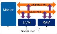
For example, the parasitic bus capacitance for one of the processor's data I/O pins is the sum of the I/O pin capacitances of the processor, the NVM and the SRAM (typically 12 pF each) and the bus track capacitance (typically 10 pF), giving a total parasitic capacitance of 46 pF. If we assume that the I/O buffer presents a 500 Ohm resistance when active, this gives a time constant, RC, of 23 ns, which is much too large for a bus using SRAM with a 10 ns access time. The only way this configuration would be acceptable would be for the bus capacitance to be reduced to less than 1 pF.
One possible solution to this problem is to let the processor access the NVM and the SRAM via separate parallel buses but this requires a large number of the processor's I/O pins. In many cases, a much more attractive solution is to use a serial NVM, as shown in Figure 2. Depending on the serial protocol chosen, the NVM will only use two or four of the processor's I/O pins. The previously-mentioned criteria for download and programming time will still be met.
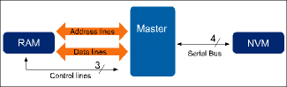
For example, consider the configuration of Figure 2 where the NVM is an ST serial Flash from the M25Pxx range. These devices have an industry standard 25 MHz SPI interface, allowing 256-byte pages to be programmed in 2 ms. Typical sector erase time is 2 s and typical bulk erase time is 3 s.
To calculate download time for 1 Mb device (M25P10, organised as 128 KB), we note that programming a 256-byte page requires only a 5-byte overhead (one for the read instruction and three for the address and one dummy one) so, with a 25 MHz clock, the time to download the whole NVM contents will be (261 x 512 x 8)/(25 x 106), or approximately 43 ms. At well below a tenth of a second, the download time will therefore be transparent to the user.
Similar calculations show that the time to initially program the memory, again using a 25 MHz clock, is 3,13 s, which is comfortably below our 5 s target. For field updates, the overall update time is the programming time (3,13 s) plus the time needed for the initial bulk or sector erase, giving acceptable update times of around 4 or 5 s.
Because they minimise loading on the SRAM data and address lines, the M25Pxx devices allow the SRAM access time to be minimised while meeting all of the other time constraints, making them ideal for code shadowing applications. In addition, all devices - including a 16 Mb device to be introduced soon - are housed in the SO8 footprint-compatible packages. The current technology allows for 0,5 Mb up to 4 Mb to be packaged in small SO8 narrow, and up to 16 Mb in MLP which is footprint-compatible.
For more information contact Avnet Kopp, 011 809 6100, [email protected], www.avnet.co.za


© Technews Publishing (Pty) Ltd | All Rights Reserved
 printer friendly version