


Fibre-optic fusion splicers are highly accurate machines which are able to automatically align and join (splice) fibre-optic cores (circa 9 µm) with sub-micron accuracy (for reference, the diameter of humanhair is ±60 µm). Splicing machines can be broadly categorised into two groups: cladding alignment vs. core alignment.
Whilst cladding alignment splicers are generally lower-cost, it is important to note that they are unable to identify the position or composition of the fibre core and subsequently line up the fibres’ outer diameters (cladding) before completing the splice.This method assumes the cores of both fibres are identical and precisely in the centre.
Core alignment fusion splicers, on the other hand, use light refraction in order to identify core types and align core positions. Thanks to the fact that glass in the fibre core and cladding have different material structure and refractive index, light passing through the core or cladding is refracted/bent differently.
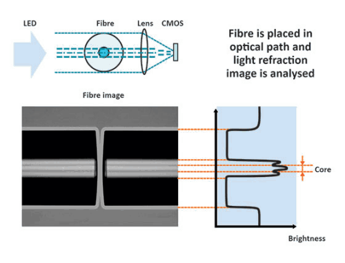
The fibre is placed within the optical path between LED light sources and CMOS detectors (Figure 1). Light, while passing through the side of the fibre on its way to the detectors, gets refracted and an image is created. Due to refraction, more light is accumulated at some points on the detector. We see some high light sections and some darker sections on the LCD display (digitally magnified a few hundred times).
The CMOS image obtained relies on the quality of the much lower magnification of the splicer’s optical components.This image is analysed, and based on the high and low light points, the splicer algorithms (the secret sauce) can identify the fibre type and know precisely where the core/cladding is.A good fusion splicer will automatically select an appropriate splice program to align and splice the fibres accordingly.This becomes especially important when joining fibres from different manufactures or types (e.g. G.652D onto G.657A1).
What is a splicer’s performance secret?
As we’ve seen, fusion splicers work based on creating and analysing images of refracted light passing through spliced fibres. Sumitomo Electric’s (SEI’s) secret is using the highest quality optical systems. Thanks to this, SEI splicers can create superior images which can be recognised and processed much more effectively. The result is that SEI devices are faster, contribute lower splice losses, and have highly accurate fibre type recognition and loss estimates. Because SEI splicers ‘see’ a lot more, they are known to handle many special fibres, sometimes with unique glass structure and refractive index profiles.
Accurate eyesight
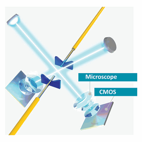
The state-of-the-art image capturing system takes ultra-precise fibre images to analyse the core position, regardless of fibre type (Figure 2).
Secret 1: Microscopes
An optimally designed microscope will have the best ‘eye’ to observe the optical fibres. The lenses are specifically designed for fusion splicing, allowing SEI splicers to offer much higher lens magnifications vs that of the company’s competitors. Do not be confused by digital magnification claims.
Secret 2: CMOS and image processing algorithm
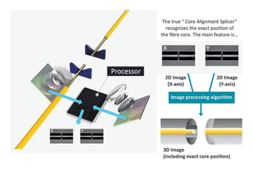
High-resolution CMOS image sensors precisely capture the image from the microscope lens. Through an ‘intelligent brain’ and superior image processing, the true ‘core alignment splicer’ recognises the exact position and profile signature of the fibre core.
The fusion splicer recognises the fibres as three-dimensional objects by processing two orthogonal fibre images (Figure 3). The intelligent, real-time image processing algorithm is the key technology which Sumitomo has cultivated as the pioneer of fibre-optic technologies.
Precise movement
The fibres are aligned with sub-micron accuracy, based on the recognised core position. Fine-tuned V-grooves and micro movement mechanisms realise core alignment at the sub-micron level. Combined with real-time image processing, the world’s quickest and finest splice is achieved.
Best materials
SEI splicers leverage Sumitomo’s group competencies as an electronic, industrial and tool materials manufacturer. Its splicers are becoming lighter and smaller, utilising high-quality materials like magnesium alloys (of which SEI is the largest global manufacturer), whereas competitors’ devices may become larger and are more often made using extremely cheap and low-quality moulded plastic parts.Superior material quality vastly reduces splicer and cleaver maintenance requirements.
Smart AI systems
Connectivity tools like SumiCloud enable access to a large volume of field splice data which, with the help of smart AI learning systems, led to the development of preventive maintenance capabilities and NanoTune advanced alignment of poorly cleaved fibres.
Sumitomo believes that the future of splicing lies with continuously improving and simplifying processes and ergonomics around the complete splicing process itself.
| Tel: | +27 12 349 1341 |
| Email: | [email protected], [email protected] |
| www: | www.lambdatest.co.za |
| Articles: | More information and articles about Lambda Test |


© Technews Publishing (Pty) Ltd | All Rights Reserved
 printer friendly version