Question: How do I add isolation to my ADC without harming its performance?
Answer: For isolated high-performance ADCs, keep one eye on isolated clocks and a second on isolated power.
SAR ADCs (successive approximation register analog-to-digital converters) have traditionally been used for lower sample rates and lower resolution. Nowadays, fast, high-precision, 20-bit SAR ADCs sampling at 1 MSps like the LTC2378-20 and oversampled SAR ADCs with 32-bit resolution like the LTC2500-32 are available. When designing for high performance to utilise the ADC performance, very low noise is required across the complete signal chain. When additional isolation is required for a signal chain, performance will be impacted.
There are three isolation topics to consider:
• Isolated power to ensure the hot side is powered.
• Data isolation to ensure the data path is isolated.
• Clock isolation for the ADC (sample clock or conversion signal), in case the clock is not generated at the hot side.
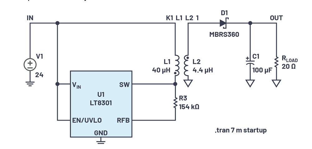 Figure 1. A typical flyback converter topology.
Isolated power (comparison between flyback and push-pull topology)
For sensor applications, isolated power is usually in a less than 10 W range.
Flyback converters are widely chosen to isolate power. Figure 1 shows the simplicity of a flyback converter. The topology’s advantage is that only a few external components are required. Flyback converters have only one integrated switch.
This switch can be the main noise source impacting signal chain performance. For high-performance analog design, the flyback converter comes with many high discontinuities in the form of electromagnetic radiation called EMI, which can limit the performance of your circuit.
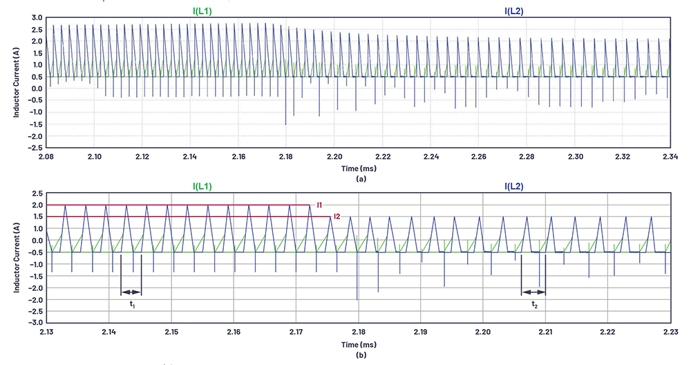
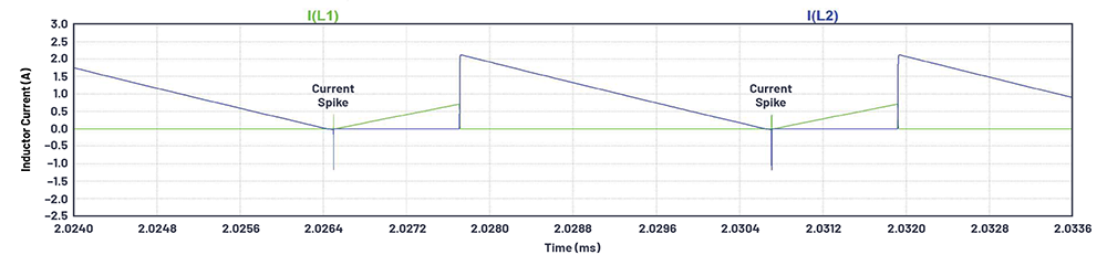 Figure 2. LT8301 switching currents in the transformer windings.
Figure 2 shows the current in transformers L1 and L2. The currents jump from high values to zero in a short period of time in the primary (L1) and secondary (L2) windings. The current spikes can be seen in the I(L1)/I(L2) traces in Figure 3. Current and energy are built up in the primary inductance and they are transferred while the switch is off to the secondary inductance, which creates transients. Those transients of the switching noise effects need to be reduced and consequently, snubbers and filters must be inserted in the design. Aside from the additional filters, an additional disadvantage of the flyback topology is that the utilisation of the magnetic material is low, leading to larger transformers due to the required high inductances. Furthermore, the hot loops of the flyback converter are large and not easy to manage.
Another challenge of the flyback converter involves the switching frequency change. Figure 3 shows a frequency change due to load change. As seen in Figure 3a, t1 < t2. This means that fSWITCH is when the load current decreases from the higher load current I1 to the lower load current I2. The variations in frequency create internal noise at unpredictable times. In addition, the frequencies will differ from part to part, which will make it more difficult to filter them as adjusted filtering would be required for each individual PCB.
Taking a 20-bit SAR ADC with a 5 V input span, one LSB corresponds to ~5 µV. The errors introduced through EMI noise should be below 5 µV, which means that a flyback topology should not be selected when isolating power for a precision system.
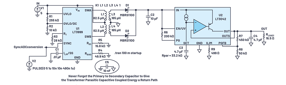 Figure 4. An LT3999 with an ultra-low-noise post-regulator.
There are other isolated power architectures with lower radiating emissions. Push-pull converters are much better suited in respect to radiation compared to flyback converters. A push-pull regulator like the LT3999 offers the possibility of clock synchronisation to the ADC and helps to achieve high performance.
Figure 4 shows the LT3999 in an isolated power circuit with synchronisation to an ADC sampling clock. Remember that the primary to secondary capacitor gives switching noise a return path to avoid common-mode noise effects. This capacitor may be realised in a PCB design with overlapping primary and secondary planes and/or with a real capacitor.
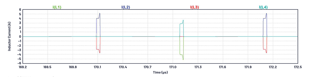 Figure 5. LT3999 current waveforms.
Figure 5 shows the current waveforms at the transformer (both the primary side and secondary side current), which gives a better utilisation of the transformer and provides better EMI behaviour.
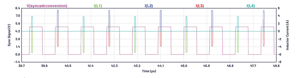 Figure 6. LT3999 and the switching relation to the sync pin.
Figure 6 shows synchronisation to an external clock signal. The end of the acquisition phase aligns to the positive edge of the sync pin. As a result, there will be a long quiet time of ~4 µs. This enables the converter to sample an input signal during that timeframe and keep the transient effects in the isolated power to a minimum. The LTC2378-20 has an acquisition time of 312 ns, which is ideal for the <1 µs quiet window.
Data isolation
Data isolation can be done with digital isolators such as those in the ADuMx family. Those digital isolators are available for many standard interfaces like SPI, I2C, CAN, etc., for example, the ADuM140 can be used for SPI isolation. To achieve data isolation, the SPI signal, SPI clock, SDO, SCK and Busy lines just need to be connected to the data isolator. In data isolation, electrical energy is transferred from the primary side to the secondary side through the inductive isolation barrier. A current return path needs to be added, which is done by a capacitor. This capacitor can be built at the PCB with overlapping planes.
Clock isolation
Clock isolation is another important task. If you want to have a high-performance ADC with 20 bits at a 1 MHz sample rate, such as the LTC2378-20, a signal-to-noise ratio (SNR) of 104 dB is possible. To achieve high performance, a jitter-free clock is required. Why shouldn’t you use a standard isolator like the ADuM14x series? The standard isolator will limit the performance of the ADC as it adds jitter to the clock.
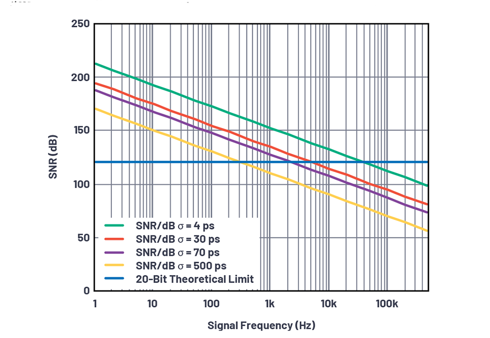 Figure 7. Clock jitter vs. ADC performance.
Figure 7 displays the theoretical limit of the SNR over frequency for various types of clock jitter. High-performance ADCs like the LTC2378 have an aperture clock jitter of 4 ps, which gives a theoretical 106 dB limit at 200 kHz input.
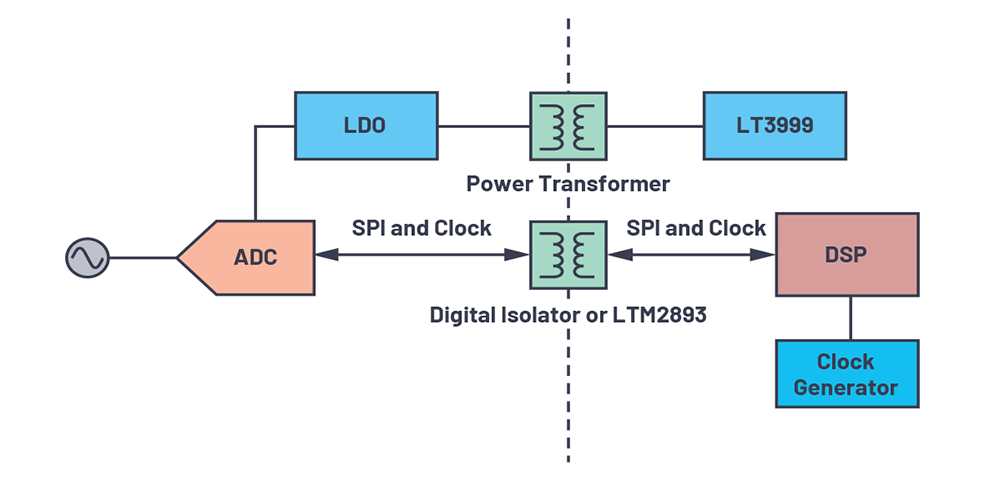 Figure 8. Clock isolation using a standard isolator.
The standard clock isolator concepts depicted in Figure 8 include:
• A good standard digital isolator like the ADuM250N has a jitter of 70 ps rms. For a 100 dB SNR goal, the signal sample rates are limited to 20 kHz due to the clock jitter.
• An optimised clock isolator like the LTM2893 provides a reduced jitter of 30 ps rms. For a 100 dB SNR goal, the signal sample rate is now 50 kHz, which gives you more bandwidth at full SNR performance.
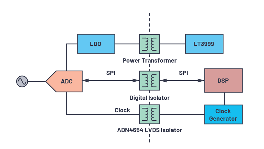 Figure 9. Clock isolation using an LVDS clock isolator.
For higher input frequencies, LVDS isolators should be used (Figure 9). The ADN4654 provides a 2,6 ps jitter, which brings you close to the best performance for an ADC. The SNR limit through clock jitter at 100 kHz input would be 110 dB.
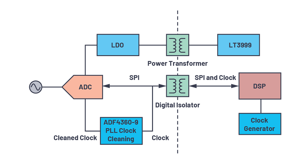 Figure 10. Clock isolation using an additional PLL for clock jitter cleaning.
Figure 10 shows the use of a PLL for clock cleaning. An ADF4360-9 can help to reduce the clock jitter.
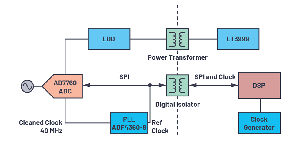 Figure 11. An ADF4360-9 used as a clock cleaner.
A more detailed block diagram for clock cleaning with a PLL is shown in Figure 11. You can use the ADF4360-9 as a clock cleaner and add a divider-by-2 to the output. The AD7760 is characterised to 1,1 MHz. A 1 MSps SAR ADC like the LTC2378 will not directly be supported. A low jitter flip-flop helps in this case as it divides the clock by 2 (Figure 12).
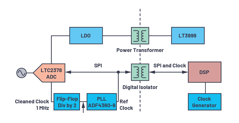 Figure 12. A flip-flop used to get the clock down for the LTC2378.
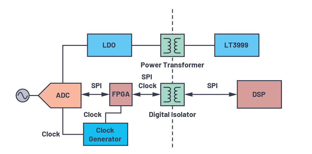 Figure 13. Clock generation at the isolated (hot) side.
As shown in Figure 13, local clock generation is another option to get a clock with the required jitter performance. Local clock generation makes the clocking architecture more complicated as it introduces asynchronous clock domains to the system. For example, if you want to use two separate isolated ADCs, the clocks will differ in absolute frequency and a sample rate conversion must be added to match the clocks again.
Clocking for high-performance sigma-delta ADCs
Similar problems with the clocks also apply for high-performance sigma-delta ADCs like the AD7760. Here the important clock signal is the jitter-free oversampling clock at, for example, 40 MHz. In this case, no additional dividers are required.
Conclusion
Isolated high-performance ADCs require a careful isolated design and a selection of various isolation techniques to achieve a high-performance SNR above 100 dB. Specific care should be taken on the isolated clock, as the influence of the clock jitter could destroy the performance. Secondly, care should be given to isolated power. Simple isolation topologies like a flyback introduce high EMI transients.
For better performance, a push-pull converter should be used. Data isolation is another, albeit less important, concern as standard available devices offer good performance and have less impact on the overall system performance. Addressing these three isolation topics enables the designer to come up with a high-performance isolated system solution.
| Tel: | +27 11 923 9600 |
| Email: | [email protected] |
| www: | www.altronarrow.com |
| Articles: | More information and articles about Altron Arrow |


© Technews Publishing (Pty) Ltd | All Rights Reserved
 printer friendly version