28 February 2022Manufacturing / Production Technology, Hardware & Services
By Sandeep Kullar, applications engineer, Nordson DAGE.
Figure 1. A range of defects that can occur during the BGA reflow process.
Ever been to see a doctor for an X-ray and/or a CT scan? This is a common process that allows medical professionals to build a complete picture for diagnosis.
In the electronics world we have similar X-ray techniques for non-destructive failure analysis. A quick 2D X-ray inspection provides a good insight into signs of defective connections and a 3D CT (computer tomography) scan can verify the problem with the added benefit of more detailed data, building the complete picture ready for diagnosis.
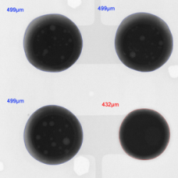
Figure 2. Ball diameter measurements performed on a BGA device.
BGA (ball grid array) packages are common devices that are inspected non-destructively utilising X-rays. Each solder joint is an individual electrical connection – a good joint will be reasonably circular in shape and the size of the joints should be reasonably consistent throughout the device array. Figure 1 shows several different types of defects which may occur during the BGA assembly reflow process.
2D X-ray inspection is a great tool for quick analysis and one type of analysis that can be easily performed is a ball diameter measurement. In Figure 2, it can be seen that the ball at the bottom right is approximately 70 µm smaller in size compared to its neighbouring joints and is highlighted with a red outline. This is the first sign that there is a potential problem with this connection.
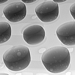
The image in Figure 3 is a 2,5D oblique-angle image of these joints. This image builds our diagnosis further, as we now see another sign that the joint in the centre is not completely fused on one side. This is seen through a different greyscale displayed on the interface of this joint and is highlighted with a red arrow.
Figure 3. 2,5D oblique-angle view of the BGA solder joints.
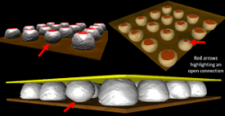
Having identified strong signs that there is potentially a defective connection, this can be verified further with a 3D CT scan. CT is a technique which captures several images from different angles and then uses reconstruction algorithms to create a 3D model. The results of this can be seen in Figure 4.
It can clearly be seen that there is a difference in the ball shape highlighted with red arrows compared with surrounding balls. The image to the top right shows the quality of ball wetting to the device interface. It is clearly seen that there is an interfacial difference compared to neighbouring joints (note the top surface of the balls, shaded in red).
Figure 4. Multiple 3D rendered views of the BGA device.
Now that both 2D and 3D images have been analysed, there is enough data to build a complete picture and diagnose this BGA device. The solder joint is confirmed as ‘non-wet open’ and the result would be a significant detrimental impact on its integrity and ultimately the integrity of the BGA device and the product it ends up in.
So, whether you are a doctor or are responsible for manufacturing quality, combining 2D and 3D X-ray images makes performing a diagnosis much easier.
Advanced X-ray inspection systems MyKay Tronics
Manufacturing / Production Technology, Hardware & Services
The Scienscope AXl-6100 series comprises specialised X-ray inspection systems explicitly engineered for the examination of long circuit boards.
Read more...Compact all-in-one placement machines Testerion
Manufacturing / Production Technology, Hardware & Services
Introducing the CLT-FG, a new series of compact all-in-one SMT placement machines
Read more...200 W of power in a space-saving design Vepac Electronics
Manufacturing / Production Technology, Hardware & Services
The Hakko FX-972 Soldering Station delivers high-performance soldering in a compact package, making it suitable for a wide range of soldering applications.
Read more...FineX: Makes shielding clear Avnet Abacus
Manufacturing / Production Technology, Hardware & Services
Panasonic Industry launches high-transparency, low-resistance, flexible transparent conductive film for electromagnetic wave shield with pre-applied OCA.
Read more...Collaboration is now critical RS South Africa
Manufacturing / Production Technology, Hardware & Services
The message emerging from RS Connect is clear: Organisations can no longer rely on internal optimisation alone to secure performance. Competitive advantage is increasingly being determined by the strength of external relationships, shared capability and coordinated action across value chains.
Read more...Disruption is the new normal. Effortless is the new competitive advantage. Seven Labs Technology
Manufacturing / Production Technology, Hardware & Services
Global supply chains have been under pressure for years. The manufacturers still standing are the ones who stopped waiting for normal to return, and started building something better.
Read more...World-first 016008 mm component placement
Manufacturing / Production Technology, Hardware & Services
Fuji has achieved the world’s first placement of 016008 mm (0,16 x 0,08 mm or 006 x 003 inches) size components on printed circuit boards with its SMT pick and place machine, NXTR.
Read more...Lifecycle and obsolescence: Protecting electronics through process Production Logix
Manufacturing / Production Technology, Hardware & Services
At Production Logix, we believe longevity is not accidental. It is engineered through early visibility, structured response, and disciplined execution, in partnership with our OEM customers.
Read more...Maximising squeegee quality and durability Testerion
Manufacturing / Production Technology, Hardware & Services
Transition Automation has announced two new product advancements designed to improve SMT printing performance and extend squeegee life: laser-enhanced Permalex bonding and integrated edge protectors.
Read more...NeoDen ND2 PCB screen printer ZETECH ONE
Manufacturing / Production Technology, Hardware & Services
The NeoDen ND2 PCB screen printing machine is a fully automatic stencil printer designed to deliver precise and consistent solder paste application in modern SMT production environments.
While every effort has been made to ensure the accuracy of the information contained herein, the publisher and its agents cannot be held responsible for any errors contained, or any loss incurred as a result. Articles published do not necessarily reflect the views of the publishers. The editor reserves the right to alter or cut copy. Articles submitted are deemed to have been cleared for publication. Advertisements and company contact details are published as provided by the advertiser. Technews Publishing (Pty) Ltd cannot be held responsible for the accuracy or veracity of supplied material.


 printer friendly version