System designers can be faced with the challenge of down-converting high DC input voltages to very low output voltages at high output current (such as 60 V down to 3,3 V at 3,5 A) while maintaining high efficiency, small form factor and simple design.
Combining high input-to-output voltage difference with high current automatically excludes a linear regulator due to the excessive power dissipation. Consequently, the designer must opt for a switching topology under these conditions. However, even with such topologies, it is still challenging to implement a design that is sufficiently compact for space-restricted applications.
Challenges faced by DC-to-DC buck converters
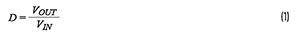
One candidate for high step-down ratios is the buck converter because it is the topology of choice when having to step down an input voltage to a lower output voltage (such as VIN = 12 V down to VOUT = 3,3 V) in an efficient way, with a significant amount of current while also using a small footprint. However, there are conditions under which the buck converter faces serious challenges to keep its output voltage regulated. To understand these challenges, we must remember that the simplified duty cycle (D) of a buck converter operating in continuous conduction mode (CCM) is:
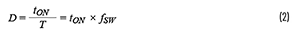
Now, the duty cycle also relates to the switching frequency (fSW) in the following way, where the on-time (tON) is the duration over which the control FET stays on during each switching period (T):
Combining Equation 1 and Equation 2 shows how tON is influenced by the step-down voltage ratio and fSW:
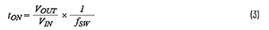
Equation 3 tells us that the on-time decreases when the input-to-output voltage ratio (VIN/VOUT) and/or fSW increases. This means that the buck converter must be able to operate with very low on-time to regulate the output voltage in CCM under a high VIN/VOUT ratio, and it becomes even more challenging with a high fSW.
Let’s consider an application with VIN(MAX) = 60 V, VOUT = 3,3 V at IOUT(MAX) = 3,5 A.
When required, we shall use values from the LT8641 regulator data sheet because a solution with the LT8641 will be provided later in this article. The required minimum on-time (tON(MIN)) corresponds to the highest input voltage (VIN(MAX)). In order to assess this tON(MIN), it is advised to make Equation 3 more accurate. By including VSW(BOT) and VSW(TOP) (the voltage drops for the two power MOSFETs of the buck converter) and replacing VIN with VIN(MAX) we obtain:
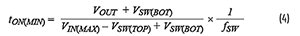
Using Equation 4 with VIN(MAX), fSW = 1 MHz, we obtain a tON(MIN) of 61 ns. For VSW(BOT) and VSW(TOP), we made use of the values provided for RDS(ON)(BOT) and RDS(ON)(TOP) in the LT8641 data sheet, knowing also that VSW(BOT) = RDS(ON)(BOT) x IOUT(MAX) and VSW(TOP) = RDS(ON)(TOP) x IOUT(MAX).
Buck converters can rarely guarantee a tON(MIN) with a short value of 61 ns obtained above; therefore, the system designer is forced to search for alternate topologies. There are three possible solutions for high step-down voltage ratios.
Solution 1: Using the LT3748 non-opto flyback
The first option consists of using an isolated topology, where the transformer performs most of the down-conversion thanks to its N:1 turn ratio. For this case, Analog Devices offers flyback controllers such as the LT3748 that do not require a third transformer winding or opto-isolator, making the design simpler and compact. The LT3748 solution for the given conditions is presented in Figure 1.
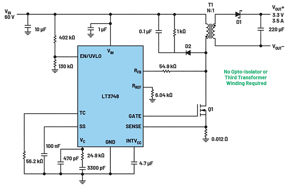 Figure 1. A circuit solution with the LT3748 down-converting 60 V input to 3,3 V output.
Even though the LT3748 solution simplifies the design and saves space compared with a standard flyback design, a transformer is still required. For applications where isolation between input and output sides is not required, it is preferred to avoid this component, which adds complexity and increases the form factor versus a non-isolated solution.
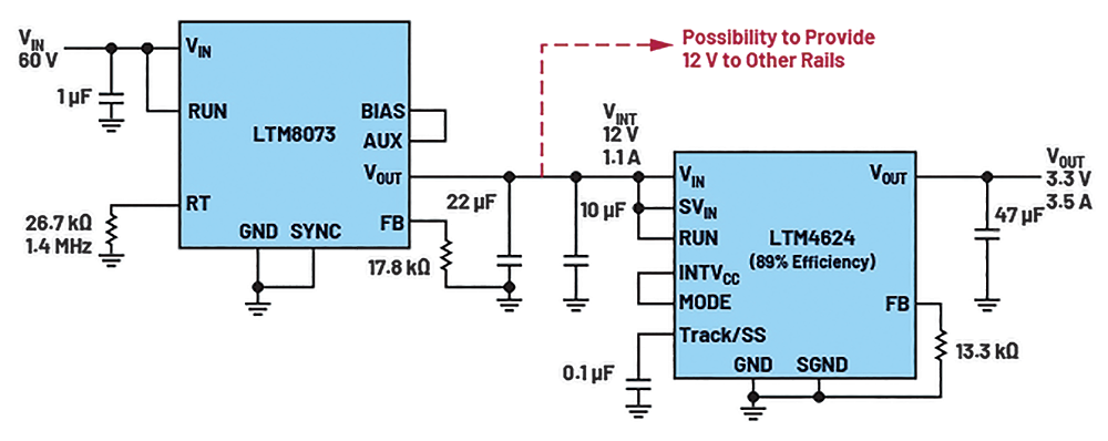
Solution 2: Using the LTM8073 and LTM4624 µModule devices
As an alternative, the designer can down-convert in two steps. To achieve a reduced component count of only 10, two µModule devices and 8 external components can be used, as demonstrated in Figure 2. Moreover, the two µModule devices already integrate their respective power inductor, sparing the system engineer a design task that is rarely straightforward. The LTM8073 and LTM4624 both come in BGA packages, with respective dimensions of 9 x 6,25 x 3,32 mm and 6,25 x 6,25 x 5,01 mm (L x W x H), providing a solution with a small form factor.
Since the LTM4624 exhibits an efficiency of 89% under these conditions, the LTM8073 supplies at most 1,1 A to the input of the LTM4624. Given that the LTM8073 can provide up to 3 A of output current, it can be used to supply other circuit rails. It is with this purpose in mind that we selected 12 V as the intermediary voltage (VINT) in Figure 2.
Despite avoiding the use of a transformer, some designers might be reluctant to implement a solution that requires two separate buck converters, especially if no intermediary voltage is required to supply other rails.
Solution 3: Using the LT8641 buck converter
Consequently, in many cases, using a single buck converter would be preferred because it provides the optimal solution to combine system efficiency, a small footprint, and design simplicity. But did we not just demonstrate that buck converters cannot cope with high VIN/VOUT combined with high fSW?
This statement might apply to most buck converters, but not to all of them. The analog Devices portfolio includes buck converters such as the LT8641, which is specified with a very short minimum on-time of 35 ns typical (50 ns maximum) over the full operating temperature range. Those specifications are safely below the required minimum on-time of 61 ns previously calculated, providing us with a third possible compact solution. Figure 3 shows how simple the LT8641 circuit can be.
It is also worth noting that the LT8641 solution can be the most efficient of the three. Indeed, if efficiency must be further optimised compared with Figure 3, we can decrease fSW and select a bigger inductor size.
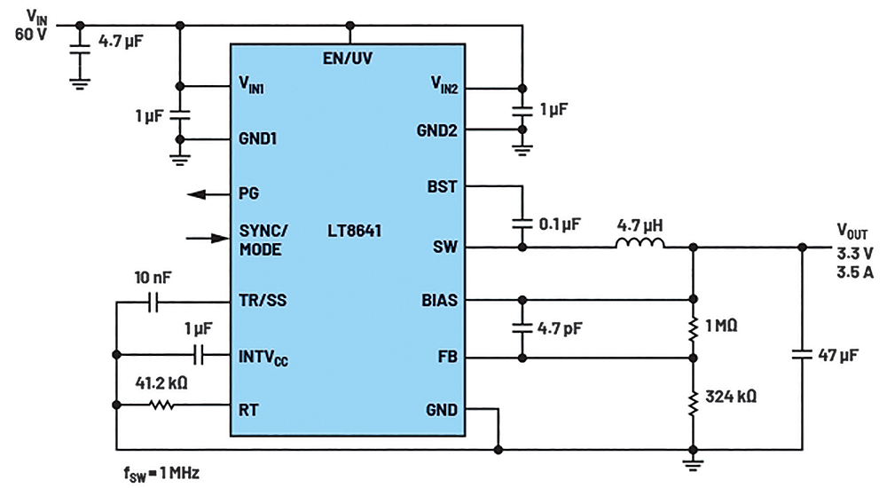 Figure 3. A circuit solution with the LT8641 down-converting 60 V input to 3,3 V output.
Although fSW can also be decreased with Solution 2, the integration of the power inductors does not offer the flexibility to increase the efficiency beyond a certain point. Moreover, the use of two consecutive down-conversion stages has a small negative impact on the efficiency.
In the case of Solution 1, the efficiency will be very high for a flyback design, thanks to its operation in boundary mode and to all components removed with the no-opto feedback design. However, the efficiency cannot be fully optimised because there is a limited number of transformers to select from, as opposed to the broad portfolio of inductors available for Solution 3.
An alternative way to check whether the LT8641 fulfils requirements
In most applications, the only adjustable parameter in Equation 4 is the switching frequency. Consequently, we reformulate Equation 4 to assess the maximum permitted fSW for the LT8641 under given conditions. By doing this, we obtain Equation 5:
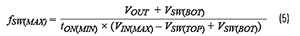
Let’s use this equation with the following example: VIN = 48 V, VOUT = 3,3 V, IOUT(MAX) = 1,5 A, fSW = 2 MHz. An input voltage of 48 V is commonly found in automotive and industrial applications. By inserting those conditions in Equation 5, we obtain:
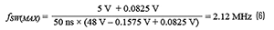
Therefore, under the provided application conditions, the LT8641 would operate safely with fSW set as high as 2,12 MHz, confirming that the LT8641 is a good choice for this application.
Conclusion
Three different methods were presented above to achieve a compact design under high step-down voltage ratios. The LT3748 flyback solution does not require a bulky opto-isolator and is recommended for designs where isolation is necessary between input and output sides.
The second method, which involves implementing the LTM8073 and LTM4624 µModule devices, is of particular interest when the designer is hesitant to select the optimal inductor for the application and/or when an additional intermediary rail must be supplied.
The third method, a design based on the LT8641 buck converter, offers the simplest and most compact solution when the sole requirement is the steep voltage down-conversion.
For more information contact Conrad Coetzee, Altron Arrow,
| Tel: | +27 11 923 9600 |
| Email: | [email protected] |
| www: | www.altronarrow.com |
| Articles: | More information and articles about Altron Arrow |


© Technews Publishing (Pty) Ltd | All Rights Reserved
 printer friendly version