How does solder reflow affect RF connectors?
EMP 2023 Electronics Manufacturing & Production Handbook
Manufacturing / Production Technology, Hardware & Services
By Janine Love, Samtec.
Solder reflow plays an important role in the success and performance of high-bandwidth RF connectors. Sometimes, when a high-bandwidth RF connector
is soldered together with an optimised PCB launch, the results can be unpredictable. It is important to investigate the root causes of solder reflow variation and analyse what techniques can deliver consistent performance across frequencies.
In a new white paper from Samtec, ‘Impacts of Solder Reflow on High Bandwidth RF Connectors,’ authors Michael Griesi (RF design & simulation engineering manager) and Chris Shelly (retired senior RF/SI modelling engineer) analyse the impact of the design choices for a specific push-on connector, its PCB, and the process. Using simulations and measurements, the team steps through its detailed development process to achieve the optimal design and better solder flow control.
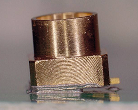
The design team began with an initial two-piece contact, traditional design shown in the image. The ‘tombstoning’ effect that was found on some of the sample connectors can be quite clearly seen, where the connectors were tilting on the PCB. Snap on connectors such as this need to stay firmly on the board, with the centre contacting the board. The initial connector design was targeting 40 GHz bandwidth when soldered onto a PCB; however, simulations showed performance of less than 25 GHz.
As a first design step, the team experimented with the thickness of the gold plating and the insulator’s coefficient of expansion. Other topics investigated include solder wicking and pooling, PCB pad design, and tuning the solder reflow process. At the end of the design process, the final design had thinner gold plating, higher temperature insulators, and a single-piece swept contact. To further address performance concerns, the team added a chamfer to the bottom of the connector, a solder control tail on the PCB pad, adjusted the thermal profile, and other process adjustments.
The performance challenges experienced with this connector design process are not unique to this type of connector. At high frequencies, every little detail matters. To achieve optimal performance, it is important to have robust simulation capabilities and multiple troubleshooting and analysis tools. The challenges of solder reflow and the impact it has on performance extends to all high-bandwidth RF connectors. At Samtec, work continues in simulation, manufacturing process, PCB and connector design to continue to optimise performance in the field of solder reflow.
Further reading:
World-first 016008 mm component placement
Manufacturing / Production Technology, Hardware & Services
Fuji has achieved the world’s first placement of 016008 mm (0,16 x 0,08 mm or 006 x 003 inches) size components on printed circuit boards with its SMT pick and place machine, NXTR.
Read more...
Lifecycle and obsolescence: Protecting electronics through process
Production Logix
Manufacturing / Production Technology, Hardware & Services
At Production Logix, we believe longevity is not accidental. It is engineered through early visibility, structured response, and disciplined execution, in partnership with our OEM customers.
Read more...
Maximising squeegee quality and durability
Testerion
Manufacturing / Production Technology, Hardware & Services
Transition Automation has announced two new product advancements designed to improve SMT printing performance and extend squeegee life: laser-enhanced Permalex bonding and integrated edge protectors.
Read more...
NeoDen ND2 PCB screen printer
ZETECH ONE
Manufacturing / Production Technology, Hardware & Services
The NeoDen ND2 PCB screen printing machine is a fully automatic stencil printer designed to deliver precise and consistent solder paste application in modern SMT production environments.
Read more...
Understanding the BGA rework process
Techmet
Manufacturing / Production Technology, Hardware & Services
BGA rework is a highly technical process that involves removing the faulty component, preparing the circuit board, and installing a new or repaired device, while maintaining the integrity of the printed circuit board.
Read more...
Flexible three-process reflow soldering system
Truth Electronic Manufacturing
Manufacturing / Production Technology, Hardware & Services
By combining multiple soldering technologies within a single system, the Vision TripleX system enables manufacturers to adapt easily to different assembly requirements, board designs, and production volumes.
Read more...
Inline vapour phase soldering for high-volume production
MyKay Tronics
Manufacturing / Production Technology, Hardware & Services
The VP2200-100 vacuum inline vapour phase soldering system from ASSCON is designed for fully automated, high-volume electronics manufacturing where process consistency and solder joint quality are critical.
Read more...
Global electronics solutions since 1964
IMP Electronics Solutions
Manufacturing / Production Technology, Hardware & Services
Over more than six decades, IMP Electronics Solutions has built a reputation for technical expertise, reliable supply chains, and strong partnerships with both customers and manufacturing partners.
Read more...
Driving excellence in electronics manufacturing
Jemstech
Editor's Choice Manufacturing / Production Technology, Hardware & Services
Jemstech’s reputation for disciplined execution and client-focused service has earned it strong loyalty from companies operating in demanding industries.
Read more...
When do you need Nitrogen in reflow?
Truth Electronic Manufacturing
Manufacturing / Production Technology, Hardware & Services
Nitrogen in reflow soldering is often seen as a performance enhancer, offering improved wetting, shinier joints, and fewer defects. But it is not always necessary.
Read more...


 printer friendly version