


When it comes to technology, most consumers get excited about products, but rarely what is inside them. However, artificial intelligence (AI) has rapidly become a colloquialism thanks to tools like ChatGPT and Midjourney. Today’s AI has matured, although slowly over three-quarters of a century, starting from research into how the brain’s neurons worked, and thinking machines in the 1940s. While much of AI’s success is down to software, it’s nothing without the hardware upon which it is developed, trained, and deployed.
Machine learning (ML) and deep learning (DL) are branches of AI that focus on statistical analysis methods and autonomous learning systems, respectively. The semiconductor industry has responded, developing tuned processors to deliver the petaflops of calculating performance these algorithms rely upon. However, there are questions around optimal memory choice, with requirements varying between training data storage, input data collected from users and sensors during operation, and intermediate results calculated during training and operation.
Data processing challenges
Of course, such processing performance comes at a price, and, in our world of democratised access to technology, it is cloud service providers that offer shared access to such AI processing power. However, AI hardware differs from the equipment needed for servers delivering websites, handling databases, and directing IoT traffic where workloads and usage demands are established and well understood. Depending on who you speak to, it is thought that a server for AI training requires twice as much SSD storage and up to six times as much DRAM than a standard cloud server. With server shipments of AI-capable hardware expected to account for nearly half of all servers by the end of the decade, that’s a significant growth in memory demand.
The challenge here is the dynamics of DRAM memory, both as a product and market. Scalability has hit a limit, meaning that we won’t get more bits per area die any time soon. Die stacking is an option but has a cost premium resulting from, among other things, challenges of yield. The goal is scalability through 3D chips, something that has changed the flash memory industry. But even if the technologies in discussion today come to fruition this decade, it will take time before they establish themselves. The market is the other issue. Prices go up and down as demand and production fluctuate, meaning that DRAM looks like the solution in one quarter but is the issue holding us back the next.
AI: Different memory for different tasks
Multiple steps must be followed before a new AI algorithm can be deployed. It starts with the data needed to train the AI. Datasets may be collections of videos taken from vehicles driving around cities, audio samples of human conversations, or images from medical scans. This information is ingested from various sources at the start of the AI data pipeline, something requiring a high throughput write-once memory (figure 1).
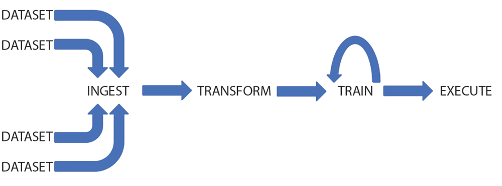 Figure 1. The AI pipeline can be broken into four stages.
Because of the disparate nature of the data, the next step in the pipeline is cleaning and transformation. Raw data is sorted and normalised to match the AI framework’s needs. Memory demands at this step vary, depending on the data in use, but speed remains critical. Due to the back-and-forth nature of the process, the read-write split can lie between 50:50 and 80:20.
Next comes the training process. The prepared data is repeatedly delivered from a storage medium to the hardware, a graphics processing unit (GPU) type processor with high-speed local memory. Over time, the algorithm improves at the task it is designed to undertake. At this stage, high-speed, read-only storage delivers data to a higher-speed memory for the duration of a learning epoch. DRAM is typically selected simply because it offers the required speed, and the compute architecture supports it. However, most of the DRAM’s task at this stage is read-heavy.
The final stage is deployment (figure 2), and the demands on memory at this point vary considerably. Users may be logging in to a server for generative AI to create images, or using a smart camera on a drone with tight demands on costs, power consumption, and weight. Either way, there has to be enough primarily read-only memory to store the AI model needed to execute its learned functionality, coupled with some read-write memory for handling intermediate and final computation results.
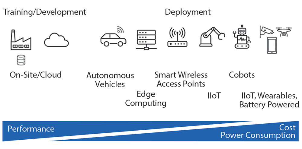 Figure 2. The rising importance of cost and power consumption after deployment.
Figure 2: While performance is the main requirement during AI training, cost and power consumption rise in importance when AI models are deployed in applications.
The gap between DRAM and SSDs
To summarise, DRAM offers high-speed, read-write data access that, generally speaking, is critical in accelerating many aspects of the AI algorithm development and deployment. However, it remains expensive per bit, power-hungry, and is overkill in many pipeline steps. SSDs, on the other hand, could be an option, especially in parts of the pipeline where data transfer is read-heavy and demands ten times lower power. M.2 and PCIe 4.0 Kioxia NVMe SSDs offer up to 7 GB/s sequential read throughputs that match DDR5-5600 bandwidths to a 10-core CPU. But the latency of flash-based disk storage (around 100 µs) is 10 000 times slower, meaning lots of wasted time waiting for data to arrive.
But a flash-based memory solution can still fill the gap between low-latency DRAM and high-bandwidth, lower-power SSDs in some cases, as researchers have found.
It’s not unusual for a training dataset to weigh in at 10 TB, meaning that many tens of servers with over 100 GB of DRAM are required to implement the training step. However, the dataset still needs to be read in from the storage medium. Researchers at MIT discovered that these disk accesses slowed the system down to speeds comparable to using flash memory. They then developed an approach combining servers with a network of FPGAs, each linked to 1 TB of flash memory. The implementation offered the same performance as a DRAM-based approach, while reducing the number of servers to ten for the same-sized dataset, significantly reducing the financial outlay.
A new memory layer – SCM
This research strengthens the voices of those promoting a new layer in the memory hierarchy. Storage Class Memory (SCM) has been proposed to bridge the gap between DRAM and flash-based storage to help ease cost pressures, without impacting performance. Targeting applications like AI that continuously access giant datasets, SCM is defined as a fully or partially non-volatile memory type providing lower read latencies than SSDs at a price point below DRAM.
Kioxia has developed XL-FLASH to target this layer in the memory hierarchy. Using a 16-plane architecture that shortens data pathways on the die, read latencies under 5 µs are attainable, ten times faster than conventional flash. XL-FLASH can be integrated into storage formats using a PCIe NVMe interface with a page size of 4 kB, rather than the 16 kB offered by a conventional flash device.
Furthermore, it is scalable, built upon multi-die packaged BiCS FLASH 3D technology, and offers the same levels of cell reliability, fast read/program times, and price-performance users have come to expect.
The remaining challenge is integrating such memory in a way that passes on as much of the latency improvements and available bandwidth as possible. NVMe uses PCIe to access block devices, but this protocol has some inefficiencies as it has to assume the data to be accessed vary in size. However, this is not the intention of SCM memory, which is proposed to be part of the memory map. Compute Express Link (CXL) is proposed as an alternative, sitting on PCIe 5 and later versions. It operates at the link layer, offering efficient access to memories and accelerators, with optional caching devices. The protocol is faster, because CXL.mem uses byte semantics to access memory, made possible because accesses are always the same size, and devices appear in the memory address space in the same manner as DRAM. Another important consideration is that both Intel and Arm processor architectures have CXL support available, so regardless of whether AI applications are deployed on servers or edge devices, XL-FLASH as a lower-cost DRAM and lower-latency flash will be an option.
Summary
While society and regulators argue about the public face of AI and how far it should encroach on our lives, the demand for AI-optimised hardware continues to grow to support the many diverse tasks it is applied to. Up until now, DRAM has been the memory of choice for servers and end applications because it is ‘how it is done’ rather than because it is the best fit.
In analysing the various steps in the AI data pipeline, it is clear that stages where the data is ‘hot’ benefit from this expensive resource, while data that is merely ‘warm’ doesn’t. SCM offers a way forward, being a midway latency point between DRAM and SSDs. When coupled with the introduction of CXL, low-latency flash, such as XL-FLASH, is well-positioned to deliver improvements in price, system performance, and power consumption to everything from servers to edge devices deploying the power of AI.
| Tel: | +27 11 236 1900 |
| Email: | [email protected] |
| www: | www.ebv.com |
| Articles: | More information and articles about EBV Electrolink |


© Technews Publishing (Pty) Ltd | All Rights Reserved
 printer friendly version