


In this article, common switch-mode power supply (SMPS) design errors will be discussed, including their appropriate rectification. It aims to address complications that arise with the power stage design of DC-DC switching regulators, focusing on the inductor.
Designers opt for inductor values outside the recommended range for various advantages, such as smaller output ripples, and minimising the solution’s footprint. However, selecting components with values that are too big or too small will result in unintended consequences that can lead to serious damage to the chip, together with decreased efficiency. This article will also examine what happens when proper care is not taken to ensure the load current does not exceed the maximum saturation rating of the inductor.
An SMPS is a highly efficient regulator that either steps down an input voltage (buck converter), steps up an input voltage (boost converter), or can do both (buck-boost converter). Basic switching converter topologies can be seen in Figure 1.
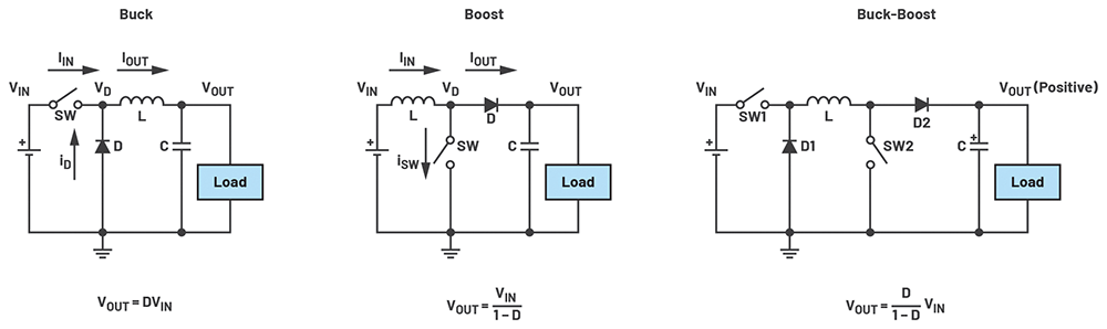 Figure 1. Common SMPS topologies.
Every SMPS works by storing energy in an inductor and utilising pulse width modulation (PWM) techniques to obtain the desired output. The guiding principle of these converters is the volt second balance law, which dictates that when operating in a steady state, over one period the average current of an inductor must be zero. This means that the inductor must discharge all the current it stored in the charging stage before another period begins.
Operation of buck converters
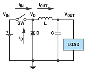
This article uses only buck converters to demonstrate common design errors. Four components make up the power stage of a buck converter: the inductor, the output capacitor, the top FET as represented by a switch, and the bottom FET, which is represented by a diode (see Figure 2).
The voltage across the inductor is given by:
The output capacitor is used to smooth out the output ripple and help maintain the desired output voltage. The output voltage of a buck converter is given by VOUT = DVIN, where D is the duty cycle, and is defined as the percentage of the time out of the total period where the top FET is on and charging the inductor.
Recommended inductor sizing
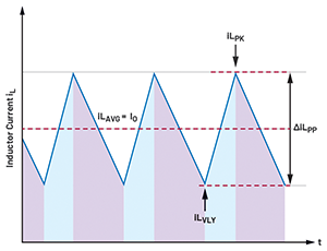
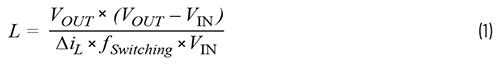
When designing an SMPS, the right inductor value must be chosen to ensure an acceptable inductor current ripple (∆iL). It is recommended that the inductor ripple should be between 30 and 40% of the applied load current for buck converters. This range is considered to be optimal, as it is big enough to capture and deliver an accurate signal to the current-mode control feedback system, but not too big that the power supply goes into discontinuous conduction mode (DCM). DCM is a state where the current ripple is too large, forcing the current to go below 0 A to maintain the load current at the desired value. However, once hitting 0 A, the diode inside the FETS no longer conducts, keeping the current from decreasing below 0 A. A general way to select the correct inductor can be obtained by the formula:
This formula shows that switching frequency and inductance are inversely proportional, meaning with higher frequencies, the charge time is reduced, allowing proper operation with a smaller inductor (saving footprint size and cost).
Saturating the inductor
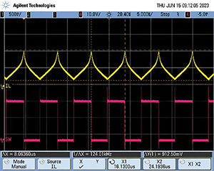
One of the most common and catastrophic errors in SMPS design is neglecting the current saturation rating when selecting the power inductor. When the current through the inductor exceeds the saturation current rating, the core of the inductor saturates, meaning that the magnetic field generated will no longer increase proportionately to the current drawn. This disrupts the volt second balance law, leading to a loss of linear characteristics in both the inductor current ripple and the output voltage ripple. When the iron core saturates, it loses inductance rapidly, behaving more as a resistor than an inductor. Since the effective series resistance (ESR) of the inductor increases, and the practical inductance decreases, the change in current is forced to increase to satisfy volts second balance. The peaking observed in the saturated current waveform is due to the exponential increase in the current slope, and can be seen in Figure 4.
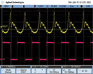
This current peaking carries over to the output voltage, leading to more noise and voltage spikes, as seen in Figure 5. The noise and voltage spikes can potentially damage downstream components if the voltage spikes too much and exceeds a downstream component’s maximum voltage rating, and can also degrade EMI performance.
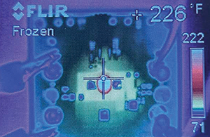
Furthermore, with high current fluctuations, the inductor experiences rapid hysteresis loss, leading to excess heat dissipation of the inductor, as seen in Figure 6, and in audible noise. This excess heat can damage other nearby components, especially the regulator chip itself.
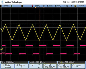
To avoid running into this issue, designers should choose inductors with a current rating at least two times greater than the expected maximum current. When calculating the maximum current, it is important to account for the inductor current ripple and the load current drawn from the output. Furthermore, designers can refer to their chosen inductor data sheet to find out at what current the inductance drops by 10 to 30% of its original value, which is where saturation is defined. Choosing an inductor with the proper saturation current rating will result in normal operation of the system, as seen by a linear current through the inductor in Figure 7. The output voltage spikes will disappear, and the system will operate at a much lower temperature, stressing the device less and improving the lifetime of the device.
For further reading please visit https://bitly.ws/3hYI
| Tel: | +27 11 923 9600 |
| Email: | [email protected] |
| www: | www.altronarrow.com |
| Articles: | More information and articles about Altron Arrow |


© Technews Publishing (Pty) Ltd | All Rights Reserved
 printer friendly version