IoT products are demanding higher frequencies and wider bandwidths than ever with varied sectors driving the demand for extreme 5G speed support in RF PCB design. These include connected vehicles, smart homes, smart cities, connected health, smart media, smart agriculture, and smart industrial applications.
Compared to 4G, 5G networks can deliver up to ten times less latency with fifty times more speed and 1000 times more capacity making it the protocol of choice for new IoT designs and products. However, key challenges in RF PCB design need to be addressed like higher frequency and wider bandwidths, multiple input and multiple output (MIMO) and beam steering, over-the-air testing, and 5G NR’s coexistence with other wireless communication systems. These challenges are amplified as product complexity increases – products are demanding smaller form-factors while simultaneously housing larger circuits.
5G specifications stipulate that handsets must support four downlink paths for bands above 1 GHz, to enable higher data rates. This requires four antennas and four independent RF pathways. For many handsets, the change will mean a substantial increase in RF content, signal-routing complexity, and antenna bandwidth. It will be challenging to squeeze even more content into already-crowded space allocated to the RF front end, and highly integrated solutions will be needed to minimise solution size and increase performance.
Antenna tuning will become even more important to keep the total number of antennas within manageable limits. In addition, increased signal-routing complexity will require the use of antenna-plexers that maximise the number of signal connections, while maintaining low insertion loss.
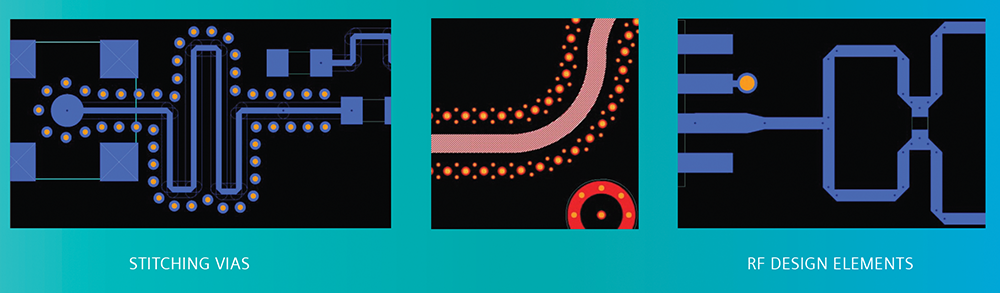
Companies wishing to take their design performance to the next level need to implement technology enablers to support their PCB design process, and designing PCBs with RF requires design features and capabilities that are specific to RF. These include:
• Ground stitching vias to shield RF circuits.
• Restrictive clearance rules specific to RF.
• Automated RF circuit arrangement and grouping.
• Meanders.
• Via-stitching for easy creation of co-planar wave guides.
• Flood regions with vias according to your rules.
• The import of complex RF shapes.
• Chamfered corners.
PCB design tools that support RF-centric design capabilities have a competitive advantage. Siemens Digital Industries Software provides you with a product design flow that puts your high-speed RF (IoT) products in a position to be ‘first-to-market’.
Designing with PCIe Spectrum Concepts
Editor's Choice Interconnection
PCI Express has become the backbone of modern high-performance systems with each new generation promising higher bandwidth, but that performance comes with a cost.
Read more...Understanding two key tools for cleaner serial data Altron Arrow
Editor's Choice Analogue, Mixed Signal, LSI
Understanding how pre-emphasis and equalisation works, and when to use one over the other, is critical when designing reliable high-speed systems.
Read more...Reliable isolation for modern networks ASIC Design Services
Computer/Embedded Technology
The Pro-Tek5 PTI Series delivers reinforced 5 kV Ethernet isolation for applications that demand robust protection, reliable signal integrity, and full IEEE802.3 performance.
Read more...Telemetry powering South Africa’s industry Interlynx-SA
Editor's Choice
As South Africa’s economy evolves, industries are under increasing pressure to improve operational efficiency and cut costs. Telemetry is becoming a vital component of industrial strategy, allowing companies to harness real-time data to optimise processes and reduce waste.
Read more...Engineering in a world that cannot assume connectivity Technews Publishing
Editor's Choice News
Across industrial automation, networking, and defence systems, engineers are rediscovering the importance of resilience and autonomy in an increasingly connected world.
Read more...Designing IoT devices for deterministic LPWAN environments
Editor's Choice Telecoms, Datacoms, Wireless, IoT
Built on Ultra Narrow Band communication technology, the Sigfox network focuses on low power, wide area M2M connectivity rather than maximising data throughput.
Read more...ARINC 429 line driver evaluation board ASIC Design Services
DSP, Micros & Memory
Holt Integrated Circuits have announced the release of the ADK-85104 Evaluation Board, a compact, ready-to-use platform designed to help engineers rapidly evaluate and characterise Holt’s HI-85104.
Read more...Driving excellence in electronics manufacturing Jemstech
Editor's Choice Manufacturing / Production Technology, Hardware & Services
Jemstech’s reputation for disciplined execution and client-focused service has earned it strong loyalty from companies operating in demanding industries.
While every effort has been made to ensure the accuracy of the information contained herein, the publisher and its agents cannot be held responsible for any errors contained, or any loss incurred as a result. Articles published do not necessarily reflect the views of the publishers. The editor reserves the right to alter or cut copy. Articles submitted are deemed to have been cleared for publication. Advertisements and company contact details are published as provided by the advertiser. Technews Publishing (Pty) Ltd cannot be held responsible for the accuracy or veracity of supplied material.


 printer friendly version