


The increasing demand for higher data rates in telecommunications and higher resolution in industrial systems is pushing the frequency of operation higher for the electronics that support them. Many of these systems operate over a wide frequency spectrum and further increased bandwidth requirements are a common request for new designs. Across many of these systems there is a push to use one signal chain for all frequency bands.
Advancements in semiconductor technology have led to breakthroughs in capability for high-power and wideband amplifiers. An area that was once dominated by travelling wave tubes has begun to cede ground to semiconductor devices thanks to the GaN (gallium nitride) revolution that is sweeping the industry and enabling MMICs (monolithic microwave integrated circuits) that generate in excess of 1 W of power over many decades of bandwidth.
As shorter gate length GaAs (gallium arsenide) and GaN transistors become available, coupled with improved circuit design techniques, new devices are becoming available that can perform comfortably to millimetre wave frequencies, opening new applications that were hard to contemplate a decade ago. This article will briefly describe the state of the semiconductor technology that is enabling these developments, circuit design considerations to achieve optimum performance, and examples of both GaAs and GaN wideband power amplifiers (PAs) that demonstrate today’s technology.
Many wireless electronic systems operate over wide frequency ranges. In the military industry, there are radar bands from a few hundred MHz to many GHz. There are electronic warfare and electronic countermeasure systems required to work over very wide bandwidth. Threats can come at a variety of frequencies, such as MHz to 20 GHz, or even higher frequencies today. As more electronics become available at higher frequencies, the need for higher-frequency electronic warfare systems will proliferate.
In telecommunications, base stations operate from 450 MHz to ~3,5 GHz and continue to increase as the need for more bandwidth continues. Satellite communications systems operate from mainly C-band to Ka-band. Instrumentation used to measure these different electronics needs to work over all required frequencies to be universally accepted. As a result, the systems engineer faces challenges trying to design electronics to cover the entire frequency range.
Given the possibility of having one signal chain cover the entire frequency range, most systems engineers and procurement folks would be very excited. There are many advantages to having one signal chain cover the entire frequency range, including simpler design, faster time to market, less component inventory to manage, and more.
The challenge with the one-signal-chain approach is always related to the performance degradation that comes with a wideband solution versus a narrowband solution. At the heart of this challenge is the power amplifier, which commonly has superior performance in terms of power and efficiency when tuned over a narrow bandwidth.
Semiconductor technology
In years past, travelling wave tube (TWT) amplifiers have dominated higher-power electronics as the output power amplifier stage in many of these systems. There are some nice attributes to TWTs, including capability of kilowatts of power, operation over octaves or even multiple octaves of bandwidth, high efficiency in back-off condition, and good stability over temperature.
There are some drawbacks to TWTs that include poor long-term reliability, lower efficiency, and the need for very high voltage to operate (~1 kV or higher). Given the long-term reliability of semiconductor ICs, there has been a push toward these electronics for many years, starting with GaAs.
When possible, many systems engineers have worked to combine multiple GaAs ICs to generate large output power. Entire companies have been created based entirely on combining technology and doing it efficiently. There are many different types of combining technologies, such as spatial combining, corporate combining, etc. These combining techniques all suffer from the same fate – combining has loss and, ideally, you would not have to use these combining techniques. This motivates us to use high-power electronics to start the design.
The easiest way to increase the RF power from a power amplifier is to increase the voltage, which has made gallium nitride transistor technologies so attractive. If we compare the various semiconductor process technologies, we can see how the power generally increases with high operating voltage IC technology.
Silicon germanium (SiGe) technology uses a relatively low operating voltage of 2 V to 3 V, but is very attractive for its integration benefits. GaAs has been used widely for power amplifiers for many years in microwave frequencies and has operating voltages of 5 V to 7 V.
Silicon LDMOS technology operating at 28 V has been used for many years in telecommunications, but it is mainly useful below 4 GHz, so it’s not as widely used in broadband applications. The emergence of GaN technology operating at 28 V to 50 V on a low loss, high thermal conductivity substrate like silicon carbide (SiC) has opened up a range of new possibilities.
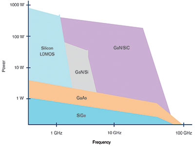
Today, GaN on silicon technology is limited to operation below 6 GHz. The RF losses associated with the silicon substrate and its lower thermal conductivity compared to SiC compromises the gain, efficiency and power as the frequency increases. Figure 1 shows a comparison of various semiconductor technologies.
The emergence of GaN technology has created an industry shift away from TWT amplifiers and a move toward GaN amplifiers as the output stage of many of these systems. The driver amplifier in many of these systems is still commonly GaAs, as much of this technology already exists and continues to be improved.
Next we will look at how to use circuit design to extract as much power, bandwidth and efficiency as possible out of these wideband power amplifiers. Certainly GaN-based designs are capable of higher output powers than GaAs-based designs, and the design considerations are largely the same.
Design considerations
There are different topologies and design considerations for the IC designer to use when choosing how to start a design to optimise power, efficiency and bandwidth.
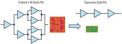
The most common type of monolithic amplifier design is a multistage, common-source, transistor-based design, also known as a cascade amplifier design. Here the gain multiplies from each stage, leading to high gain and allowing us to increase output transistor sizes in order to increase the RF power. GaN offers benefits here because we are able to greatly simplify the output combiners, reducing loss and thereby improving efficiency, as well as shrinking the die size, as shown in Figure 2. As a result, we are able to achieve wider bandwidths and improve performance.
A less obvious benefit of going to GaN devices from GaAs is to achieve a given RF power level, perhaps 4 W – the transistor size will be less, resulting in a higher gain per stage. It will lead to fewer stages per design and ultimately higher efficiency. The challenge with this cascade amplifier technique is that it is difficult to achieve bandwidths over an octave without significantly compromising the power and efficiency, even with the help of GaN technology.
Lange coupler
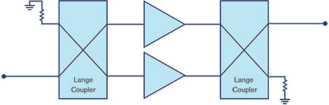
One approach to achieve wide bandwidth design is to implement a balanced design with Lange couplers on the RF input and output, shown in Figure 3.
Here the return loss is ultimately dependent on the coupler design, as it becomes easier to optimise the gain and power response over frequency without also needing to optimise the return loss.
Even while using Lange couplers, it becomes more difficult to achieve bandwidths over an octave, but they do offer a very nice return loss for the design.
Distributed amplifier
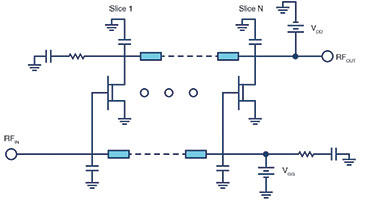
The next topology to consider is the distributed power amplifier shown in Figure 4. The benefit of a distributed power amplifier is accomplished by incorporating the parasitic effects of the transistor into the matching networks between devices.
The input and output capacitances of the device can be combined with the gate and drain line inductance, respectively, to make the transmission lines virtually transparent, excluding transmission line loss. By doing this, the gain of the amplifier should only be limited by the transconductance of the device and not the capacitive parasitics associated with the device.
This only happens if the signal travelling down the gate line is in phase with the signal travelling down the drain line, so that each transistor’s output voltage adds in phase with the previous transistors output. The signal travelling to the output will constructively interfere so that the signal grows along the drain line. Any reverse waves will destructively interfere since these signals will not be in phase.
The gate line termination is included to absorb any signals that are not coupled to the gates of the transistors. The drain line termination is included to absorb any reverse travelling waves that could destructively interfere with the output signal and improve the return loss at low frequencies. As a result, multiple decades of bandwidth are able to be realised, from kHz to many GHz.
This topology is popular when more than an octave of bandwidth is needed and there are some nice benefits, such as flat gain, good return loss, high power, etc. An illustration of a distributed amplifier is shown in Figure 4.
One challenge with distributed amplifiers is that the power capability is dictated by the voltage applied to the device. Since there is no narrowband tuning capability, you are essentially providing a 50 Ω impedance to the transistor (or close to it). When we consider the equation for average power out of a power amplifier – POUT = VDD2/(2 x RL) – RL (or optimum load resistance) essentially becomes 50 Ω. Therefore, the achievable output power is set by the voltage applied to the amplifier such that if we want to increase the output power, we need to increase the voltage applied to the amplifier.
This is where GaN becomes very helpful, as we can quickly go from a 5 V supply voltage with GaAs to a 28 V supply voltage in GaN, and the achievable power goes from 0,25 W to almost 8 W simply by changing from GaAs to GaN technology. There will be other considerations to look at, such as the gate length of the process available in GaN and if they can achieve the gain you need at the high-frequency end of the band. As time progresses, more of these GaN processes become available.
The fixed RL of 50 Ω for distributed amplifiers is different compared to the cascaded amplifier where we change the resistance value presented to the transistor by matching networks to optimise the power from the amplifier. There is a benefit in optimising the resistance value presented to the transistor with cascade amplifiers in that it can improve the RF power.
Theoretically, we can continue increasing the transistor periphery size to continue increasing the RF power, but there are practical limitations to this, such as complexity, die size and combining loss. The matching networks also tend to limit the bandwidth, as they become difficult to provide an optimum impedance over wide frequencies. In the distributed power amplifier, there are only transmission lines whose purpose is to have the signals constructively interfere along the amplifier, rather than matching networks.
There are additional techniques to further improve the power in distributed amplifiers, such as using a cascade amplifier topology to further increase the voltage supply to the amplifier.
Today’s product capability
We have shown that there are various techniques and semiconductor technologies that offer trade-offs in providing optimum power, efficiency and bandwidth. Each of these different topologies and technologies will likely have a place in the semiconductor world, as they each provide benefits, which is why they have survived to this day. Here we’ll focus on a few results that we believe show what is possible with these technologies today to achieve high power, efficiency and bandwidth.
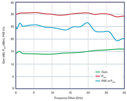
The Analog Devices HMC994A is a GaAs-based, distributed power amplifier operating from DC to 30 GHz. This part is interesting because it covers many decades of bandwidth, lots of different applications, and achieves high power and efficiency. The performance is shown in Figure 5. Here we see a saturated output power covering MHz to 30 GHz with over 1 W of power and a power added efficiency (PAE) of 25% nominal.
This particular product also has a strong third-order intercept (TOI) performance of 38 dBm nominal. This result shows that with GaAs-based designs we are able to achieve an efficiency that is close to what is possible with many narrowband power amplifier designs. Given the positive gain slope with frequency, high PAE, wideband power performance, and strong return loss make the HMC994A an interesting product.
It’s also interesting to see what is achievable with GaN-based technology. Analog Devices offers a standard product, HMC8205BF10, which is based in GaN and combines high power, efficiency and bandwidth. This product operates from a 50 V power supply and provides 35 W of RF power at 35% nominal efficiency with ~20 dB of power gain covering over a decade of bandwidth.
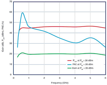
In this case, a single IC is able to provide roughly 10 times more power compared to similar approaches in GaAs. In years past, this would have required a complicated combining scheme of GaAs die that would not have been able to reach the same efficiency. This product demonstrates what is possible with GaN technology covering wide bandwidths and providing high power and efficiency, as shown in Figure 6. It also shows progress in high-power electronic packaging technology, as this part is housed in a flange package capable of supporting continuous wave (CW) signals needed for many military applications.
Summary
The emergence of new semiconductor materials like GaN has opened the possibilities to reach higher power levels covering wide bandwidths.
Shorter gate length GaAs devices have extended frequency ranges from 20 GHz to 40 GHz and beyond. The reliability of these devices is shown in literature to exceed 1 million hours, making them ubiquitous for modern day electronic systems. We expect the trends of higher frequencies and wider bandwidth to continue into the future.
| Tel: | +27 11 923 9600 |
| Email: | [email protected] |
| www: | www.altronarrow.com |
| Articles: | More information and articles about Altron Arrow |


© Technews Publishing (Pty) Ltd | All Rights Reserved
 printer friendly version