


QFN (quad flat no lead) and LGA (land grid array) and other bottom mounted parts were introduced to industry a few years ago and their use has increased significantly in many industry sectors. The cost to produce these packages is more cost effective than their leading alternatives, they take up less space, and are more robust in assembly.
Like any new package, they do introduce new challenges to assembly staff. It is important to run trials and make design, assembly and quality staff aware of any special requirements before running in high volume. Always have a procedure in place for good new product introduction (NPI)
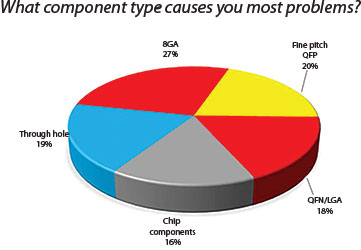
A recent webinar survey of 100 engineers shows that QFN/LGA parts are a common cause of process problems for users; however BGA (ball grid array), QFP (quad flat package) and through-hole still create more issues (refer to Figure 1).
The main point of discussion with these parts is voiding, which may not be an issue to all users. More recent use in more demanding environments has also illustrated that long-term thermal cycling performance may still be an issue due to cracking of edge joints. This is due to the difference in expansion rates between the package and PCB. The larger the package in terms of lead count, the bigger the problem.
The following is a brief synopsis of assembly defects that can occur with these components, and should help newcomers and expert users alike. A full copy of the 30-page defect guide, complete with photographs, is available free of charge – see contact details at the end of this article.
QFN and LGA are the most common terms used in industry to describe these types of components, and have been around since they were first introduced around 2000. Other names and abbreviations have been used but often by marketing departments to differentiate their company’s parts from the rest. The IPC standard ‘IPC 7093 Design & Assembly Process Implementation for Bottom Termination Components’, first introduced in 2011, tried to use one common term to avoid confusion: Bottom Termination Component (BTC).
Satisfactory solder joints
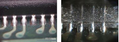
Both the images in Figure 2 show satisfactory solder joints formed during reflow, with good wetting to the side terminations. There is no requirement for solder fillets to the side of the parts under IPC standards due to the lack of wetting on these parts during their early introduction. Some vendors have been successful in improving their process, changing the singulation method or changing the lead frame and plating steps.
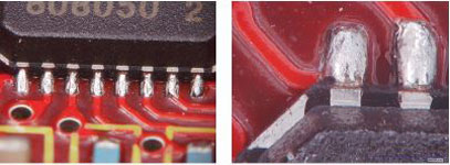
The solder joints in Figure 3 are again satisfactory, with reduced wetting on the side lead frame which is typical of parts that do have some level of side solderability. Having designs that allow formation of side solder fillets allows for automatic optical inspection (AOI) and easier rework and repair, touch up of single joints, and is good practice. The formation of side fillets may also slightly improve the reliability during temperature cycling.
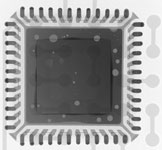
The X-ray image in Figure 4 shows an example of what would be considered satisfactory soldering of a QFN package with minimum voids under the centre pad or in the outer pads. The image was created by Dr David Bernard and the author in the first guide to X-ray inspection and published by Dage in 2006 during the introduction of lead-free soldering.
Failure of QFN joints
Solder joint failure (Figure 5) may occur for several reasons, including differential thermal expansion of board and component; flexure or dropping testing substrates; and coating/encapsulate expansion.
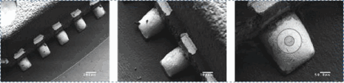
The rate that solder joints have been found to fail is due to thermal expansion of the solder alloy, joint height, temperature range, size of package, and size of die in package. These reasons for failure also relate to the design of the product and the thickness of the substrate.
To confirm product reliability for a specific environment, engineers do need to undertake some reliability assessments on any new component types and alloy combinations. The scanning electron microscope images in Figure 5 were taken after 1000 cycles between 125°C and -55°C with no apparent visual damage. Microsections did detect some level of cracking in selected joints.
A full copy of the 30-page defect guide, complete with photographs, is available free of charge, and includes further topics such as tin plating slivers and burrs, poor termination solderability, uneven termination plating, solder paste reflow with vias, solder joint failure and laminate cracking, voids in solder joints, open solder joints, solder balls/balloons, solder beads, solder squeeze out, inconsistent solder joint volume, poor conformal coating adhesion, no-clean flux residue, dendrite formation, and solder balls and beads. In addition, the author is providing all of his colour process defect guides plus two textbooks on pin-in-hole reflow and package-on-package assembly.


© Technews Publishing (Pty) Ltd | All Rights Reserved
 printer friendly version