


The overall cost to produce a completed printed circuit board (PCB) can be broken down into several basic categories: the cost of manufacturing the blank PCB, the cost of components, the assembly costs, and the cost of test. That last one, the cost of testing the completed board, can comprise as much as 25% to 30% of the total cost of producing the product.
Two logical aspects make up design for profitability: design for manufacturability (DFM), that is, developing a product at the lowest possible manufacturing cost while maintaining the lowest rate of defects, and design for testability (DFT). By designing a product to have the highest test coverage and the ability to isolate faults quickly regarding both manufacturing errors and component failures, DFT becomes paramount in designing for profitability. This article explores DFT in depth, and specifically looks at in-circuit testing (ICT).
DFM and DFT guidelines
When selecting a contract manufacturer (CM), they should always provide DFM and DFT guidelines. Always make sure you get and read these guidelines for each CM you are considering. Reviewing the DFM and DFT guidelines from different CMs may provide insight into each one’s level of expertise, knowledge and capability. Consequently, these guidelines are a helpful tool when deciding which CM is the best fit to produce your company’s products.
Planning ahead
The first questions to ask when planning a design are 1, who is going to test the assembly? and 2, what are their capabilities?
The DFT guideline will be helpful in the initial planning of the layout. However, it is a good idea to contact the CM directly and discuss your specific needs with a knowledgeable test engineer. The test engineer will be able to discuss their capabilities and make you aware of the different test methodologies they’re able to provide.
A combination of a boundary scan (JTAG), automated ICT test, X-ray laminography (AXI) and visual inspection (manual and machine vision) will provide the most comprehensive test coverage. It will also give you access to immediate feedback on the manufacturing process so that workflow can be quickly adjusted as needed, and defective components can be spotted and rejected.
Next, you should consider what test coverage is necessary to guarantee a quality finished product. Utilising the full arsenal of test capabilities available may or may not be required for your application, and in fact, may be cost prohibitive. For example, if you are fielding a one-of-a-kind satellite orbiting earth, you will want to perform every type of test available, to ensure that the finished product will function reliably for years in an environment where repair is not an option. However, if you are producing musical greeting cards, a simple, functional test may be all that is required.
ICT test
ICT testing can detect a number of defects, on both the manufacturing and component fronts. There are two types of ICT test systems. One system utilises a test fixture, which clamshells the printed circuit assembly (PCA) under test and probes various nets to perform the test. The second is a flying probe test, where the probes are controlled by a computer system to make electrical contact with specific nets of the PCA under test.
Some of the things which can be tested for include shorts/opens, missing components, components placed with the wrong polarisation or even the wrong value, and a number of other aspects. ICT testers can also power the PCA under test and exercise analog and digital circuits to verify proper operation. ICT test systems can perform this regimen of tests with a high volume throughput.
Design considerations for ICT testing
The requirements are slightly different for what can be considered a test point for ICT testers employing test heads vs. the flying probe test.
For test systems using a test head, there will be DFT guidelines that dictate the features of a test point. As you map the placement and layout of the PCB, be sure to have a copy of that DFT guideline on hand, from the CM who will be doing the final assembly testing.
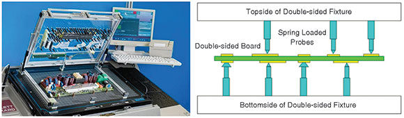
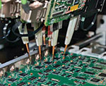
The ICT fixture (Figure 1) will probe various features on the board, to make measurements and provide power, stimulus, and measure signals on the PCA under test. Test systems can probe both sides of the PCA. However, keeping the test points to one side of the board will decrease the complexity of the test fixture, resulting in a lower cost and higher return on investment (ROI) for the product.
Once a test fixture has been developed for a PCA, any additional modifications to the test fixture to facilitate changes to the product will result in extra costs. These additional costs can add up. Therefore, care must be exercised when making any modifications to the PCA, to not move any of the existing test point locations.
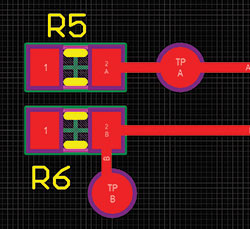
Many features of a PCA can be utilised as an ICT test point. There are different types of spring-loaded probes (pins) to facilitate making a proper electrical connection to a net on the PCA. Through-hole pads which have a lead protruding can often be probed, such as connector pins protruding onto the secondary side (bottom) of the board. Vias can often be used as test points. However, SMT pads with soldered components attached may not be considered a valid test point when a test fixture is employed.
Where SMT technology is applied, and there are no available vias to use as test points, test point pads must be incorporated into the design. The geometry and clearance of the ICT test pad should be among the items covered in the DFT guidelines provided by the CM performing the testing. Other relevant information which the DFT document will provide includes clearances between test points, clearance to the edge of the board, and what can be used as a test point.
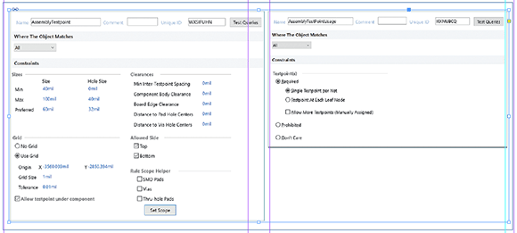
The EDA tool used to perform the layout of the board will have a set of design rules (Figure 3) to define what constitutes a test point, along with the required test coverage. By properly configuring these sets of rules (according to the DFT guidelines) in the planning stages of layout, producing the test documentation will become an automated process.
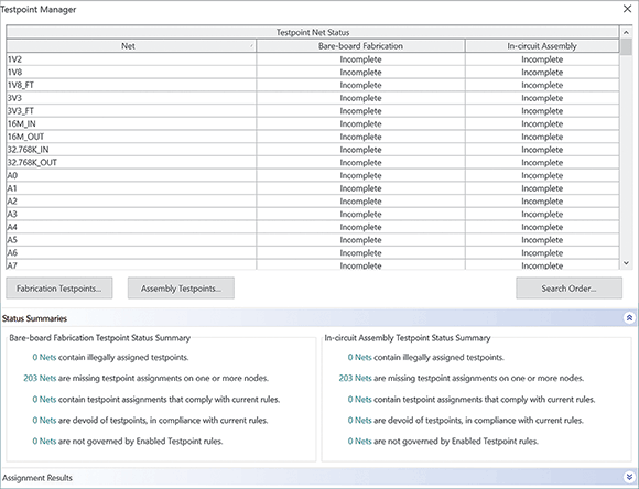
Once the test point design rules have been configured, the EDA tool will have automated features to assign the test points in the design, as shown in Figure 4. Generally speaking, the documentation produced will be a test point file or report, containing the coordinates of each test point. This report may be generated in a variety of file formats, including the IPC-D-356A format. Other file formats may be required by the CM performing the test or creating the fixture. Consult with your testing CM to verify what data is required to produce the test fixture.
Flying probe test
The flying probe tester (Figure 5) does not require tooling for a test fixture, and will therefore be the lowest-cost ICT testing solution. Additionally, soldered SMT component leads on the PCA may also be probed. When vetting the CM to perform ICT testing, it may be prudent to ask if they have flying probe ICT test capabilities. This will only require programming of the test system and not tooling costs to produce the test fixture. Additionally, engineering changes (ECO) to the PCA will not require avoiding changes to the test points, as any differences between the old and new assembly will only require programming changes.
Conclusion
With the testing phase of a completed circuit board comprising up to 30% of overall costs, it’s more important than ever to fully plan and strategise your DFT process. This begins with knowing the capabilities of your manufacturer and what test coverage is considered necessary to guarantee a quality finished product. Once your planning phase is finalised, a comprehensive ICT test will allow you to detect a number of defects before your board is fully manufactured.
For more information contact EDA Technologies, +27 (0)12 665 0375, [email protected], www.edatech.co.za
| Tel: | +27 12 665 0375 |
| Email: | [email protected] |
| www: | www.edatech.co.za |
| Articles: | More information and articles about EDA Technologies |


© Technews Publishing (Pty) Ltd | All Rights Reserved
 printer friendly version