


When it comes to automatic optical inspection (AOI) everyone is talking about 3D. But is this technology just marketing hype, or is it the real answer to the heightened demands being placed on soldered printed circuit board (PCB) inspection?
The fact is that smaller components and increasing component densities are creating an even bigger challenge for AOI systems to face. Demands for first-pass yield, that is, the yield after the first production run, are becoming stricter since rechecking of unnecessarily rejected PCBs is expensive and time consuming.
The development process has reacted to this: throughput has increased, image quality has improved, and cameras featuring an additional angled view and software algorithms for fully automated image evaluation have made defect detection a much more reliable process.
What is more, 3D technology brings new insights, making actual height information available for evaluation for the very first time. So how important is this information, and how reliably is it recorded? How should X-ray inspection be classified in this context?
Inspection technologies compared
Product defects during the automated assembly and soldering of electronic assemblies are unavoidable. More and more, systems for AOI and automated X-ray inspection (AXI) are being deployed to assure these defects are detected and to further optimise the process.
Frequently, these systems are employed for post-reflow inspection, since they offer the greatest potential for quality improvement after this process step. Various technologies are used for this:
* Cameras with orthogonal (vertical) top views (AOI, 2D technology).
* Cameras with an additional angled view (AOI, 2D technology).
* Height measurement of the board with components (AOI, 3D technology).
* X-ray inspection (AXI, 2D, 2.5D or 3D technology).
Until a few years ago, automatic optical inspection was almost exclusively a 2D technology. These 2D processes have continually improved, and systems featuring angled cameras ensure a high level of process quality. They are able to combine high inspection speed with very good, robust defect detection while achieving a low pseudo-defect rate.
Genuine 3D processes, featuring actual height measurement and volumetric measuring, used to be too inaccurate, expensive and slow. But further technical development of the sensors and evaluation hardware has allowed various genuine 3D technologies to make inroads into AOI. Depending on the technology, this permits height measurement for components, IC pins and solder joints.
Types of defects and the ability to identify them
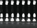
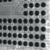
Inspection of assembled and soldered components can reveal many types of defects, which can be caused by individual production steps, paste print, assembly and soldering. These include the absence of components, displacement and twisting, polarity, incorrect components, lack of solder or insufficient solder, thick solder joints, bent or upright IC pins (lifted leads), solder bridges and inadequate wetting (dewetting or tombstoning).
These basic types of defects have been known for more than 25 years. Additionally, components are getting smaller and smaller (0201, 01005, 03015), and IC types such as the ball grid array (BGA) with smaller and smaller pitch (0,8, 0,5, 0,4) are being employed in the automatic production process. Moreover, new components such as LEDs, quad flat no-leads (QFN), connectors and other special designs are also employed.
The increased component density on electronic assemblies and other influences lead to smaller and smaller connection pads. These trends increase the defect spectrum: chip lifted leads in all angles, ICs/BGAs that are not coplanar (if no X-ray inspection is conducted), poor wetting on QFNs and dual flat no-leads (DFN), non-coplanar plugs, bent plug pins, relational measurement, measurement tasks (LEDs), colour analysis, head in pillow on BGAs (only with X-ray inspection) as well as additional solder and wetting errors on individual, concealed solder joints.
Most of these types of defects can be found reliably and with high throughput using modern, high-quality 2D AOI. For some (extended) types of defects, this is only partially true.
Strengths and limitations of 2D technology
Today, 2D AOI inspection is state of the art. Highly sophisticated, it is a reliable method for carrying out post-reflow inspection. However, the technical features offered by the systems available on the market differ in many respects, including camera resolution (in μm/pixels), size of the camera sensor (number of pixels), field of view resulting from the resolution and camera size, frame rate (number of images per second), presence of angled cameras, acquisition of full-resolution colour images (three colour separations with a full number of pixels), algorithm-based image processing or image comparison, and multi-coloured illumination from as many directions in space as possible.
The better the individual features, the better the overall AOI performance, which is determined by the throughput, defect detection (as few undetected defects as possible are desirable) and pseudo-defect rate. Besides image quality, which is supposed to display the defects so they are clearly recognisable, the software (algorithm-based image processing) has a key role to play. The better the algorithms used for fully automated defect evaluation, the easier it is for the user to make the correct defect detection settings.
For 2D technology, angled-view cameras are a particularly important means of obtaining good inspection results about defect features. This includes achieving full sharpness and depth of field across the entire field of view – something that is possible if intelligent solutions are used. The market has recognised that the angled view provides significantly more information compared to pure vertical inspection.
Equipped with good camera technology and software, 2D systems offer a wide range of performance features: inspection of all visible solder joints including gullwing ICs, optical character recognition, data matrix code reading, straightforward recognition of certain polarity marks, high throughput, reasonable costs, relatively few problems resulting from shadowing, and multiple solutions for additional tasks beyond solder joint inspection, such as measurement tasks or colour analyses.
However, 2D technology also has its limits. For example, it cannot perform inspection of hidden solder joints or measurement of connectors (straight alignment for later automatic joining). Furthermore, optimisation of defect rates for certain defect features is possible only with comparatively expensive means, while direct evaluation of 3D data is not possible and higher pseudo defect rates occur for some defect features.
3D technology
The newer 3D technology has been used for some time in surface mount technology (SMT) production for inspection of paste print after the screen printer. Now, it is also being successfully used for post-reflow inspection. For the first time, actual height information can be obtained and additional defect features detected.
Components not on the same level and bent leads are detected. Also for the first time, additional features involving height can be inspected. Basic features, such as the presence of components, can finally be checked more easily and pseudo defects reduced.
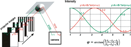
The 3D processes used in post-reflow inspection had long been too imprecise, expensive, slow and not sturdy enough. Meanwhile, 3D technology can also be reliably used for inspection of soldered electronic assemblies. Here, the moiré multi-frequency process using multi-phase shift (known as fringe projection method) has largely won out. In this process, structured light patterns with different frequencies are projected into the field of view. In turn, for every frequency used, various phase lengths are projected, whereby each phase shift depicts a specific part of the wavelength.
Despite this, 3D technology also has some drawbacks and limitations: More work is involved in the process of defect detection, which drives up associated costs. Technological limitations include the fact that many basic defect features, such as a number of polarity marks and characters, cannot be identified.
In addition, data matrix codes are not read in 3D; colour information is lacking; the edges under the components are not analysed (PLCC and Melf, for example); more shadowing problems occur; throughput is reduced; there is no evaluation of hidden solder joints with classification of each individual joint (e.g. on the QFN or BGA); and high components can only be inspected to a limited degree.
Use of automated X-ray inspection
X-ray inspection has proved its value especially for evaluating hidden solder joints. There are also many devices in the market that work with 2D or 3D technology. Here, too, 3D technology offers some advantages – inspection of printed circuit boards populated on both sides – but also has some disadvantages, such as markedly higher costs and lower throughput.
In any case, X-ray inspection permits evaluation of every individual solder joint. In 3D inspection with AOI, a non-coplanar BGA produces a message for the entire component only. There are also other defect features of hidden solder joints that do not show up in tilting of the component. These include the head in pillow, but also voids in solder joints or solder bridges between solder joints.
Summary: 2D and 3D technology
This newer 3D technology will succeed. It eliminates some method-related disadvantages and, by obtaining more information, increases reliability of results. But 3D technology cannot and will not replace 2D technology. While it is opening up new technology horizons, it cannot do everything better than 2D technology – and indeed, in some cases it falls far short.
In particular, it is often impossible to ensure alignment with the criteria of IPC-A-610 due to the presence of combined conditions or the requirements for only ‘visibly good wetting’. Consequently, it makes sense to use 3D technology in AOI contexts as an addition to 2D technology, in much the same ways as X-ray inspection can enhance AOI inspection. After all, what matters is not the technology used, but whether the right inspection result is obtained.
Where AOI is concerned, using a combination of 2D and 3D technology is the way to ensure better detection of all visible defect features. Assuming that 3D technology is implemented correctly, many defect features can be directly recorded and reliably detected. This is particularly true for tilted components and bent leads. This requires a software platform that not only provides all the necessary evaluation algorithms with a high level of quality, but is also able to flexibly combine the possibilities offered by 2D and 3D technology in a way that exploits their strengths.
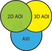
The ideal solution is to use various elements from the 2D AOI, 3D AOI and AXI toolkit to build tailored solutions that meet customer-specific requirements – and for a single manufacturer to do this. Combining the various options available in this way can considerably improve both inspection quality and user processes.
| Tel: | +27 11 824 1427 |
| Email: | sales@techmet.co.za |
| www: | www.techmet.co.za |
| Articles: | More information and articles about Techmet |


© Technews Publishing (Pty) Ltd | All Rights Reserved
 printer friendly version