


Integrating mechanical design workflows into electrical design tools has become a necessary component of today’s successful PCB design processes. But transferring inaccurate design data back and forth between the ECAD (electronic computer-aided design) and MCAD (mechanical computer-aided design) worlds can not only cause frustrations felt by both design teams but can also drastically increase the number of design spins required to fit the PCB into its final assembly. Regardless of the electrical design tool’s 3D capabilities, accurate component 3D modelling information is crucial to the success of this process.
What is the issue here?
The MCAD tools traditionally supply all mechanical data. Some use antiquated methods like DXF or IDF files to exchange that data. While IDF can be useful in creating simple extrusions of component bodies, many details are missed because of the limitations of the IDF file. STEP model integration provides a significantly higher level of three-dimensional data that can not only be passed over to the MCAD world but can also be used directly in your ECAD tool.
Integration methods for STEP models can differ between toolsets. It is important that the model can be easily imported into the footprint while also having the ability to be visually manipulated in the 3D environment. Having to switch between the native PCB tool and a different 3D viewing environment can add yet another hurdle to this process.
Solution
Adding and manipulating 3D models in a native 3D design environment like Altium Designer makes the unification of the ECAD and MCAD worlds as efficient as possible. The following sections will explain how to obtain 3D STEP models and embed them in your PCB design environment.
Obtaining models
The first step in adding a 3D model to a footprint is obtaining the model, but where from? There are several methods available. One of the first choices should be internal to your organisation. Your mechanical design team may have already created the 3D models for your electronic components, so why look any further? If they haven’t, it may be a simple process to get them built.
Most MCAD toolsets can export to the STEP format (either AP-203 or AP-214 are supported in Altium Designer). One advantage of having your MCAD team create these models is the 3D component can be built to your exact specifications, including specifying which of a package’s min/typ/max sizes to use, orientation, origin point, colours, etc. Additionally, any modifications or corrections can be made quickly and easily.
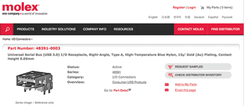
Another avenue is to visit a part manufacturer’s website. Many component companies will make STEP models (and other file formats) available, usually for free. This is especially true of components that have a detailed mechanical aspect to them, like connectors. Figure 1 shows an example of a USB 3.0 receptacle from Molex.
Other online resources exist: one great example is 3D ContentCentral. This is an online user and supplier community that is hosted by Dassault Systèmes (the creators of SOLIDWORKS). It includes thousands of supplier and user-created part models.
Any user-uploaded model has a rating assigned to it by the user community, so you can be confident in the quality and accuracy of the 3D model you are downloading. Depending on how the model was uploaded to the site, multiple download formats may be available in addition to STEP. Verifying the model with your organisation’s MCAD team is, however, recommended.
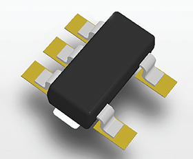
Altium Designer itself can also create STEP models for components created using the IPC compliant Footprint Wizard. Figure 2 is an example of a 5-pin SOT23 package generated directly inside an Altium Designer .PcbLib file.
Embedding models
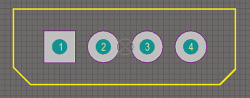
Once the STEP model has been created or downloaded, adding it to the footprint is a straightforward process. For this example, we’ll be using another Molex connector – the 15-24-4449 power connection header. The 2D land pattern has been created in the Altium Designer .PcbLib file as shown in Figure 3.
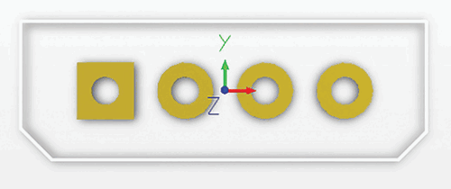
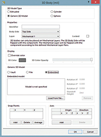
Switching to 3D mode (View » 3D Layout Mode) as shown in Figure 4 will make adding and manipulating the STEP model easier. Next, select Place » 3D Body, to open the 3D Body dialog. In the dialog, set the 3D model type to ‘Generic 3D Model’ and confirm that the generic 3D model type is set to ‘Embedded’. Then, click the ‘Load from file...’ button. You’ll then browse to the location of the downloaded STEP model and select ‘Open’.
Clicking OK in the 3D Body dialog will load the STEP model into the .PcbLib workspace attached to your cursor as shown in Figure 6. Using the keyboard hotkey combination of ‘J’ (Jump) and then ‘R’ (Reference) snaps the cursor (and the attached STEP model) to the reference, or zero-zero point, of the footprint. Hitting ‘Enter’ places the model at its destination.
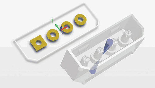
This model was imported under an ideal scenario. The orientation of the STEP model matched the orientation of the 2D footprint perfectly and the origin point of the 3D model was at the same centre point as in the footprint. The STEP model didn’t need any manipulation before placing it correctly in the footprint.
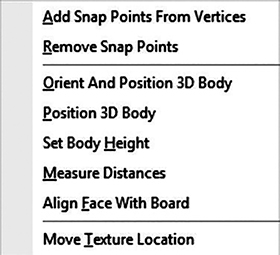
There may be situations when the STEP model wasn’t created using the same orientation as the footprint, or a height adjustment needs to be made, so it sits flat on the board surface. Altium Designer has many features available in the 3D design mode created specifically to assist in the dynamic manipulation of the STEP model so that it lines up correctly with respect to the land pattern as shown in Figure 7.
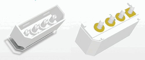
After a ‘Save’ is performed on the .PcbLib file, this 2D/3D footprint model is now ready to be used in any PCB design. Accurate component body to component body (as well as component body to enclosure) clearance and collision checking can now be performed right within Altium Designer. In addition, a STEP export of your PCB file will now include this detailed model information, which can be read by almost any MCAD toolset.
Conclusion
By using STEP models in your ECAD tool, it’s possible to get data-rich and accurate 3D models that can easily be exchanged between ECAD and MCAD worlds. And with accurate 3D STEP models being used to confirm enclosure fits, you will have successfully reduced the number of required design spins while ensuring that your board fits right the first time.
| Tel: | +27 12 665 0375 |
| Email: | [email protected] |
| www: | www.edatech.co.za |
| Articles: | More information and articles about EDA Technologies |


© Technews Publishing (Pty) Ltd | All Rights Reserved
 printer friendly version