By Zhen Feng, Juan Carlos Gonzalez, Sea Tang, Murad Kurwa, Evstatin Krastev, Nordson Test & Inspection.
Figure 1. BGA DMN-8802 dual encoder processor.
The electronic manufacturing industry needs non-destructive techniques to identify BGA opens and cracks. Currently X-ray and time domain reflectometry (TDR) are most widely used.
This whitepaper reports the results of a comparison of the following techniques: TDR, automatic X-ray inspection (AXI), transmission X-ray (2DX), cross-section/SEM, and Dye & Pry. The first three are non-destructive, while the cross-section/SEM and Dye & Pry are destructive techniques.
A correlation among the various techniques in finding opens and cracks in BGA joints were looked at. The experiment included:
• Testing thirty pins on a particular BGA from ten different boards using TDR, AXI, and 2DX.
• Further examining eight of those boards with cross-section/SEM, and the remaining two boards with Dye & Pry.
These studies helped gain a good understanding of TDR, AXI, 2DX, cross-section/SEM and Dye & Pry techniques.
Introduction
More BGA and area array devices are appearing on PCBAs as product/functional complexity increases. Furthermore, to achieve good signal integrity, more I/Os are packed in smaller areas within the available real estate. Therefore, engineers need non-destructive techniques to identify BGA defects when ICT or FT calls for a faulty device. Identifying BGA cracks is not an easy task with the available tools including 2DX. Automatic X-ray inspection (AXI) systems are used for identifying BGA opens in electronics manufacturing, however, it is challenging for AXI Laminography to detect BGA defect size less than 4 mils.
Time Domain Reflectometry (TDR) has the capability to identify BGA full cracks (opens) using impedance measurement data. The 2DX has been widely used to identify BGA defects because of its clear image. Engineers often use cross-section/SEM or Dye & Pry to identify defective BGA pins; however, the boards are destroyed during these tests. Because of this, non-destructive techniques were studied to look for a correlation with the cross-section/SEM and Dye & Pry methods.
AXI has more than 90% coverage for PCBA, and is an effective tool for collecting real time data for SMT process improvement. Engineers usually use 2DX to verify critical defective BGA pins found with the AXI. Both AXI and 2DX are non-destructive techniques, and so is TDR. Thus, TDR, AXI and 2DX was chosen for this study. The objective was to find the correlations between the different testing methods:
• TDR, SEM, and Dye & Pry;
• 2DX, SEM and Dye & Pry;
• TDR and 2DX.
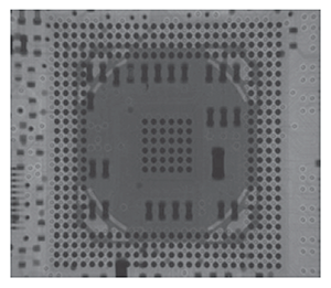
Equipment used for the comparison work were a LeCroy WE100H mainframe with ST-20 TDR module, an Agilent Laminography 5DX, a Dage XD7500 transmissive X-ray, and a JEOL Scanning Electron Microscope. These are TDR, AXI, 2DX and SEM, respectively. The BGA DMN-8802 Dual Encoder processor has defects based on ICT and FT testing, and was selected as the object of the experiments.
The BGA is on a board which is a Set-Top Box bundled with user-controlled broadcast, frame enhancement, and network access. The fab, which has six layers, has 388 pins with a pitch size of 0,75 mm. Thirty BGA pins were selected for the experiment including A24 and C26. Solder joint problems have been reported previously for A24 and C26 using SEM and Dye & Pry.
Outscale your competition
Manufacturing / Production Technology, Hardware & Services
Attendees will be able to explore the benefits of AMD Kintex UltraScale+ Gen 2 FPGAs in high-performance Pro AV, test & measurement, industrial, and medical applications.
Read more...MTN SA Foundation drives youth pathways into the digital economy
Manufacturing / Production Technology, Hardware & Services
The MTN SA Foundation, in partnership with Helios Towers and Datacomb Development Hub, has launched the MTN–Helios Towers 12-month ICT Learnership Programme, a pathway that takes young South Africans from digital training into real workplace experience.
Read more...The impact of harsh environments and ionic contamination on post-reflow circuit assemblies MyKay Tronics
Manufacturing / Production Technology, Hardware & Services
There is well documented historical proof that post-reflow circuit assemblies, when subjected to harsh environments, are particularly vulnerable to failure mechanisms, but modern electronic assemblies are far more susceptible to this phenomenon.
Read more...Engineering copper grain structure for high-yield hybrid bonding in 3D packaging Testerion
Editor's Choice Manufacturing / Production Technology, Hardware & Services
The way copper grains are sized and distributed forms the metallurgical foundation of hybrid bonding, enabling lower bonding temperatures, greater reliability, and stable grain structures throughout integration.
Read more...Understanding solder dross: causes and control strategies Truth Electronic Manufacturing
Editor's Choice Manufacturing / Production Technology, Hardware & Services
Dross formation is an inevitable consequence of wave soldering. It occurs when molten solder comes into contact with oxygen, forming metal oxides that float on the surface of the solder bath. Over time, this oxidation byproduct accumulates and must be removed to maintain solder quality and process consistency.
Read more...Implications of using Pb-free solders on X-ray inspection of flip chips and BGAs MyKay Tronics
Manufacturing / Production Technology, Hardware & Services
With the move to Pb-free soldering, most of the attention has been paid to reflow temperatures, component compatibility, and reliability concerns, but the implications for inspection, particularly X-ray inspection, are equally important and often underestimated.
Read more...The causes of solder balls in robotic soldering
Manufacturing / Production Technology, Hardware & Services
Solder balls (also known as solder splatter) are a major concern in many production sites as they may potentially cause shorts, leading to long-term impacts on product reliability.
Read more...Material challenges for superconducting quantum chips
Manufacturing / Production Technology, Hardware & Services
To achieve the scalable and repeatable production of superconducting circuits for quantum technology products, players in the industry are leveraging semiconductor fabrication techniques.
Read more...UV curing oven for high-efficiency PCB production Techmet
Manufacturing / Production Technology, Hardware & Services
The jCURE-2UV+ from JTU is a cutting-edge ultraviolet curing oven engineered for fast, reliable curing of UV-sensitive coatings in SMT production environments.
While every effort has been made to ensure the accuracy of the information contained herein, the publisher and its agents cannot be held responsible for any errors contained, or any loss incurred as a result. Articles published do not necessarily reflect the views of the publishers. The editor reserves the right to alter or cut copy. Articles submitted are deemed to have been cleared for publication. Advertisements and company contact details are published as provided by the advertiser. Technews Publishing (Pty) Ltd cannot be held responsible for the accuracy or veracity of supplied material.