


Visual examination of ball grid array (BGA) solder joints is best achieved using an endoscope system, which are available from a number of suppliers worldwide. These systems have been specifically designed to allow solder joints to be examined between the base of the device and the printed circuit board (PCB).
Often there are limited stand-off heights and overhang restrictions due to the body of the package. The close proximity of components to the body of the device to be examined may also limit the opportunity for inspection, particularly when scanning along the sides of devices. With care, design engineers can always leave areas free of parts, particularly on the corners of adjacent sides of a device.
Although not covered in this article, X-ray criteria are available, and this is the popular alternative to optical inspection. X-ray was of course the first choice for BGA inspection when area array devices were first introduced, and is commonly used in industry. The author has conducted many hands-on training courses on inspection criteria for both optical and X-ray inspection, and produced the first training videos and interactive CD-ROM on area array inspection
It is possible to examine the outer row of ball terminations with traditional inspection equipment, depending on stand-off height and the overhang on the side of the BGA. However, this is not feasible to use on inner ball terminations or where the overhang obscures the terminations when tilting the board assembly.
Both X-ray and these specialist inspection systems have limitations on the process issues and defects they can detect. If the budget is available, the ideal situation is to have both methods of controlling and defining the manufacturing process, or to have samples from production examined by an external source.
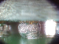
Ideally some visual standards should be provided for operator reference during final inspection or during process monitoring. This is true for both X-ray and optical inspection, as assessing joints can be daunting for staff members new to these techniques. Criteria should include conventional BGA, chip scale package (CSP), package on package (POP) and flip chip terminations with tin/lead or lead-free eutectic and high-temperature ball terminations. Solder joints to high temperature terminations do look different! – see Figure 2.
Examples of the soldering quality on high-temperature balls often featured on ceramic ball grid arrays (CBGA) should be included due to the difference in surface appearance. With balls that become liquid with the paste, there is little evidence of any demarcation between the two solder surfaces. With high-temperature balls like 90%lead/10%tin there will be a demarcation line between the solder alloy and the ball. This is because the ball does not reflow but the paste does. There can be differences in the height the solder rises up the ball due to the paste volume and the wettability of the terminations. The line formed at this point has often been referred to as the waist line and mistakenly referred to in some specifications as defective.
In cases where lead-free termination BGAs are used with tin/lead paste, the ball may not completely reflow at 210°C – 225°C. These temperatures are quite normal for a surface mount assembly with tin/lead. Tin/silver/copper (Sn/Ag/Cu) or SAC balls will have a reflow temperature of approximately 217°C. As new alloys are used on area array packages to improve shock and drop performance the problems can become more complex.
If measurements are to be taken during inspection then the following can be used as a guide. It is good practice to take some measurements on typical BGA devices during early production runs or the first new product introduction (NPI) build against specific devices and their locations. If problems do arise in future production these measurements can be very useful for reference and for comparing reworked devices.
Remember that the measurements here are only a reference, as the final dimensions will depend on the original ball size on the device, the paste thickness and pad surface on the board. In the case of reworked devices, it matters whether paste was used for replacement, or flux-only reflow.
Size of ball terminations
Ball diameter should be equal to or larger than the original ball diameter on the BGA prior to reflow, due to the addition of paste. In the case of high-temperature lead/tin ball terminations which do not reflow, there should be no change in ball size. The ball size does define the stand-off height of the package.
Stand-off height of BGA package
Measure the difference in height between the board and the base of the BGA laminate on a minimum of two of the four corners. Compare the variation in height of the BGA by scanning along the length of the BGA on two sides. The height will be equal to or less than the original ball height. The stand-off height will reduce due to the size of the device and its weight.
Variations in height between the centre and the edges of the BGA may indicate warpage of the fibre glass device or PCB. It can also indicate voiding in the ball terminations. This is more commonly noted if all termination measurements are taken. Warpage can occur up or down in the centre area of the part, although uncommon warpage can even be seen on ceramic packages.
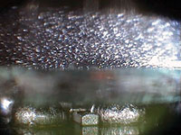
Check for solder shorts
Scan along two adjacent sides of a BGA using light from the opposite side of the devices. There should be no restrictions to viewing each of the termination outlines. If light is restricted, short circuits may be visible under the device. Viewing two sides makes sure that shorts can be seen, whereas shorts can be missed when viewing one side only. Also look for chip components under packages due to poor placement control.
Check for complete reflow of solder paste and ball terminations on tin/lead or lead-free joints. In the case of high-temperature balls on ceramic parts, the ball will not become liquid. During soldering the paste will reflow and allow wetting to take place between the high-temperature ball and the pad surface. There will be a distinct line between the ball and the solder at the interface. This is due to the different metal surfaces being joined.
Summary
BGA failures do occur for a variety of reasons; they may be component, printed board, process or design related. On some occasions, both X-ray and optical inspection cannot easily provide the answer and that is when other techniques must be used. Microsections, dye penetrant and acoustic scans may assist is pinpointing the root cause.
The essential aspect in all analysis is the experience of the engineer who is tasked with finding the root cause of the failures. There is no substitute for practical experience.
For more information visit www.bobwillis.co.uk


© Technews Publishing (Pty) Ltd | All Rights Reserved
 printer friendly version