


There are many different routes to an ASIC and all kinds of trade- offs have to be considered at the outset of a design, in opting to do either an initial design in programmable logic, with a conversion to follow, or to go straight to an ASIC. Considerations of device size, projected volume, time-to-market and risk, will all feed into the decision-making process, which takes place against a background of constantly evolving technology.
This article takes an up-to-date look at some of the trade-offs, and helps place in context a new service from Actel that claims to take away some of the risk and time-to-market issues that keep many away from the standard cell ASIC approach.
While the trajectory of programmable logic has certainly been upward in recent years, with improvements in price, performance, and design tools suited to an ever wider range of applications, recent months have seen harsher assessments of the technology's contribution to many designs, with respect to the bill of materials. As certain sectors of the industry take stock of the need to cut costs, the value of time-to-market is waning in the eyes of many - at least for the time being - and with it the reticence of some to consider ASICs.
Recent months have seen a renewed enthusiasm for FPGA-to-ASIC conversion, with program announcements from most of the major programmable logic vendors, as well as the arrival of many smaller players, and all are providing conversions to the older gate array ASIC technology.
Benefits
A major benefit of taking the FPGA-to-ASIC route is that there is no need to wait several weeks or months for silicon to be ready, designers of the system can get on with prototyping and debugging the design. Time-to-market and risk are the two factors that stop many from using ASICs. In the first case, designers can expect to take anything from eight to 16 weeks to go from specification to production, with longer times being needed in the event of problems or a re-spin. The greater NRE charges, now in the domain of over US$1m for 0,18 µm designs, make ASICs a risky undertaking, with there being little room for error should a re-spin be needed or worse, the target market collapses or changes and the manufacturer is left with a huge inventory of useless ASICs.
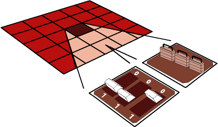
The attraction of going for an initial design in FPGA, then moving to an ASIC once uncertainties have been ironed out and volumes have ramped, is therefore obvious. All of the conversion programmes on offer today lead the design to a gate array ASIC, with the exception of Actel's recently announced ProASIC FPGA-to-ASIC service, which converts to the higher density standard cell ASIC. The key features of this option are summarised in Figure 1.
The cost trade-offs have always favoured a move from an FPGA to a gate array ASIC as the number of gates and volume of devices increases. Recent years have seen the cost gap between the FPGA and gate array narrowing somewhat, to the extent that there is now virtually no price difference between the two at lower gate densities, favouring the use of FPGAs in ever-larger volumes. A 10K ASIC gates (30K FPGA gates) FPGA cost around US$50 three years ago but today it's under US$5. The equivalent gate array would have been around US$5 three years ago compared with US$3 today, a price difference with much less impact on the bill-of-materials.
Intense demand for increasingly complex devices is fuelling the growth of standard cell ASICS, whereas gate arrays are unable to satisfy the requirements of such complex designs. As a result, manufacturers are changing the emphasis from gate arrays in favour of standard cell ASICS for larger gate count requirements. Unlike gate arrays, which have a predefined structure (with customisation carried out via the deposition of one or two final metal layers), standard cells are fully customisable with few limitations on size or layout, making them considerably more size efficient. Designers using standard cells have more of an opportunity to make optimal use of the chip, not being constrained to choosing from a set of predefined layouts with fixed options in terms of size and on-chip elements. A designer looking for a gate array with an ARM core on it, for instance, will likely have a more arduous search for a vendor and a suitable device, and even then may have to contend with a memory provision that is not exactly what was wanted, with less than optimal use of the chip.
So there are a number of factors driving the migration to standard cell, which is now well underway, but it has nonetheless remained impractical to convert from an FPGA to one of these designs, the technologies being so fundamentally different in structure.
Planting a flag in this uncharted territory Actel is now coming on-line with a service that offers conversion from its flash based ProASIC FPGA to, uniquely, a standard cell ASIC, potentially eliminating the risk and time-to-market bugbears that put many off the standard cell approach. The service comes with similar NREs to other standard cell offerings, of the order of US$150K, which are payable once a customer has made a commitment to an ASIC, and so is an option only open to those with the projected volumes and the demanding size and density requirements to make standard cell worthwhile. A big difference to the other conversion schemes however is the fact that the ProASIC FPGA has been designed from the bottom-up to be similar to an ASIC in structure, thereby ensuring a clean and simple conversion process, as shown in Figure 2.
SRAM-based FPGAs have an architecture that, compared to an ASIC, is very coarse-grained. They are made up of elements called configurable logic blocks (CLBs) which typically consist of two look-up tables (LUTs) and a flip-flop. More effort has to be put into mapping from this LUT-based structure to the cell structure of a gate array where the basic element is a two input NAND gate.
Problems typical with the process include timing headaches, difficulties in predicting utilisation and performance, and the fact that the choice to eventually move to a gate array has to be made early on -when the design is still at the FPGA stage. Another problem that can occur when converting to a gate array based ASIC is the possible discrepancy in supply voltages, with the older gate array technology sometimes being a generation behind the FPGA, presenting the need for extra conversion of voltage levels in the system design.
Actel's Pro-ASIC FPGA avoids problems arising from the conversion to ASIC by using a basic three-input/one-output cell structure that is very similar to the two-input/one-output cell of a standard cell ASIC. This makes it very easy to map designs between the two. The similarity in cell structures means the ProASIC can be designed using exactly the same design flow as an ASIC. The ProASIC cell comprises around nine gates, compared to the 100 or so gates that make up a CLB in an SRAM FPGA. One potential drawback to using such a fine-grained structure is that many more switches are needed to carry out the same function in ProASIC cells as could be carried out with a CLB, like using smaller bricks to build a house. However, being flash-based, the switches can be made with just two transistors on the ProASIC, rather than the eight transistor SRAM cell that is needed to implement a switch on an FPGA. There is, therefore, room to implement many more switches without sacrificing too much die area.
SRAM FPGAs also make for an uneven transition to ASICs in the sense that the PCB design will be different, as SRAM FPGAs require nonvolatile memory to boot-up the FPGA when the system starts up. The circuit has to be configured to ensure that nothing happens until this has taken place, circuitry that would then be redundant should the design move to an ASIC. Being flash based, the ProASIC requires no extra circuitry or power-up and is a single chip design, so the system can be designed exactly as it would be with an equivalent ASIC.
A customer wishing to convert a design from ProASIC to standard cell would initially supply their netlist, pin assignments, functional test vectors and timing constraints. The standard NRE covers a series of steps from netlist conversion (optional) and re-synthesis into the 0,25 µm standard cell technology to fabricating a finished prototype. Optional stages in-between include: scan insertion, automatic test pattern generation (ATPG), BIST and JTAG interface. Also covered under the basic NRE are the development of factory test-vectors and a test program, mask fabrication and prototype fabrication. Additional charges are made for things like extra ATPG, should the customer not be entirely happy with the test coverage, as may happen in more complex designs, costs an extra US$10K.
Summary
Actel's ProASIC-to-ASIC conversion programme forms another interesting piece in the puzzle for designers weighing up the tradeoffs inherent in the multitude of FPGA, ASIC and conversion programmes on offer today. It is certainly the first scheme to promise a removal of the risk and time-to-market issues that weigh heavily on the minds of many of those considering the standard cell approach. Looking to the wider horizon, the signs are that gate arrays will continue to diminish as a viable option for many designs, with many of those that would have taken this approach in the past now migrating to standard cells, at the higher density end of things, while FPGAs continue to eat away at the lower density gate array business.
For further information contact Kobus van Rooyen, ASIC Design Services, (011) 315 8316.
| Tel: | +27 11 315 8316 |
| Email: | [email protected] |
| www: | www.asic.co.za |
| Articles: | More information and articles about ASIC Design Services |


© Technews Publishing (Pty) Ltd | All Rights Reserved
 printer friendly version